AD9364
Data Sheet
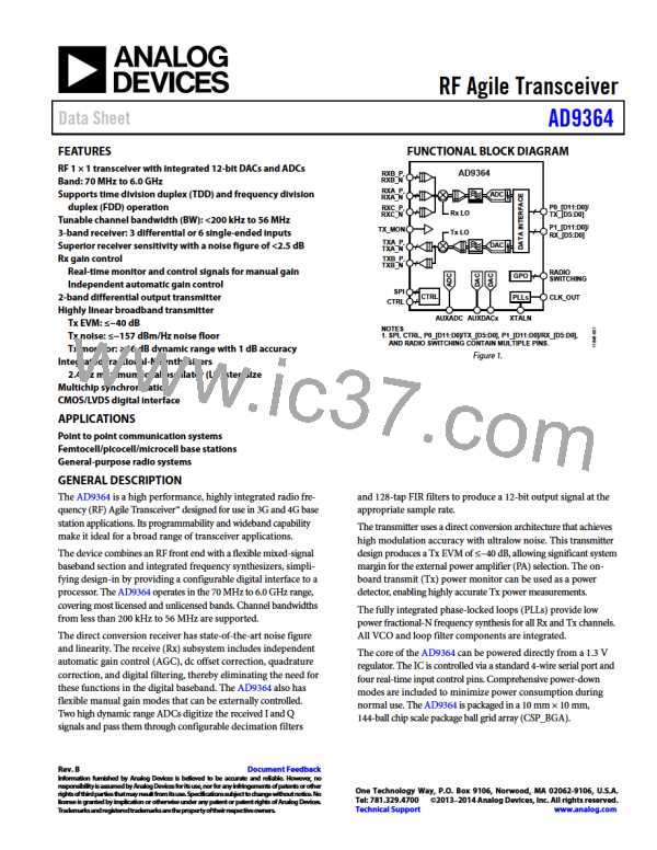
THEORY OF OPERATION
GENERAL
TRANSMITTER
The transmitter section consists of two differential output stages
that can be multiplexed to the transmit channel. The transmit
channel provides all digital processing, mixed signal, and RF
blocks necessary to implement a direct conversion system. The
digital data received from the BBP passes through a fully
programmable 128-tap FIR filter with interpolation options. The
FIR output is sent to a series of interpolation filters that provide
additional filtering and data rate interpolation prior to reaching the
DAC. Each 12-bit DAC has an adjustable sampling rate. Both
the I and Q channels are fed to the RF block for upconversion.
The AD9364 is a highly integrated radio frequency (RF)
transceiver capable of being configured for a wide range of
applications. The device integrates all RF, mixed signal, and
digital blocks necessary to provide all transceiver functions in a
single device. Programmability allows this broadband transceiver
to be adapted for use with multiple communication standards,
including frequency division duplex (FDD) and time division
duplex (TDD) systems. This programmability also allows the
device to be interfaced to various baseband processors (BBPs) using
a single 12-bit parallel data port, dual 12-bit parallel data ports,
or a 12-bit low voltage differential signaling (LVDS) interface.
When converted to baseband analog signals, the I and Q signals
are filtered to remove sampling artifacts and fed to the upcon-
version mixers. At this point, the I and Q signals are recombined
and modulated on the carrier frequency for transmission to the
output stage. The combined signal also passes through analog
filters that provide additional band shaping, and then the signal
is transmitted to the output amplifier. The transmit channel
provides a wide attenuation adjustment range with fine granularity
to help designers optimize signal-to-noise ratio (SNR).
The AD9364 also provides self calibration and automatic gain
control (AGC) systems to maintain a high performance level
under varying temperatures and input signal conditions. In addi-
tion, the device includes several test modes that allow system
designers to insert test tones and create internal loopback modes
that can be used by designers to debug their designs during
prototyping and optimize their radio configuration for a
specific application.
Self calibration circuitry is built into each transmit channel to
provide automatic real-time adjustment. The transmitter block
also provides a Tx monitor block. This block monitors the
transmitter output and routes it back through the receiver
channel to the BBP for signal monitoring. The Tx monitor
block is available only in TDD mode operation while the
receiver is idle.
RECEIVER
The receiver section contains all blocks necessary to receive RF
signals and convert them to digital data that is usable by a BBP.
It has three inputs that can be multiplexed to the signal chain,
making the AD9364 suitable for use in multiband systems with
multiple antenna inputs. The receiver is a direct conversion
system that contains a low noise amplifier (LNA), followed by
matched in-phase (I) and quadrature (Q) amplifiers, mixers,
and band shaping filters that downconvert received signals to
baseband for digitization. External LNAs can also be interfaced
to the device, allowing designers the flexibility to customize the
receiver front end for their specific application.
CLOCK INPUT OPTIONS
The AD9364 operates using a reference clock that can be provided
by two different sources. The first option is to use a dedicated
crystal with a frequency between 19 MHz and 50 MHz connected
between the XTALP and XTALN pins. The second option is to
connect an external oscillator or clock distribution device (such as
the AD9548) to the XTALN pin (with the XTALP pin remaining
unconnected). If an external oscillator is used, the frequency
can vary between 10 MHz and 80 MHz. This reference clock is
used to supply the synthesizer blocks that generate all data
clocks, sample clocks, and local oscillators inside the device.
Gain control is achieved by following a preprogrammed gain
index map that distributes gain among the blocks for optimal
performance at each level. This can be achieved by enabling the
internal AGC in either fast or slow mode or by using manual
gain control, allowing the BBP to make the gain adjustments as
needed. Additionally, each channel contains independent RSSI
measurement capability, dc offset tracking, and all circuitry
necessary for self calibration.
Errors in the crystal frequency can be removed by using the
digitally programmable digitally controlled crystal oscillator
(DCXO) function to adjust an on-chip variable capacitor. This
capacitor can tune the crystal frequency variance out of the
system, resulting in a more accurate reference clock from which
all other frequency signals are generated. This function can also
be used with on-chip temperature sensing to provide oscillator
frequency temperature compensation during normal operation.
The receiver includes 12-bit, Σ-Δ ADCs and adjustable sample
rates that produce data streams from the received signals. The
digitized signals can be conditioned further by a series of
decimation filters and a fully programmable 128-tap FIR filter
with additional decimation settings. The sample rate of each
digital filter block is adjustable by changing decimation factors
to produce the desired output data rate.
Rev. B | Page 28 of 32

 ADI [ ADI ]