AD8615/AD8616/AD8618
TYPICAL PERFORMANCE CHARACTERISTICS
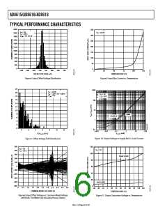
2200
350
300
250
200
150
100
50
V
= 5V
S
V = ±2.5V
S
2000
1800
1600
1400
1200
1000
800
T
= 25°C
A
V
= 0V TO 5V
CM
600
400
200
0
0
–700
–500
–300
–100
100
300
V)
500
700
0
25
50
75
100
125
OFFSET VOLTAGE (
μ
TEMPERATURE (°C)
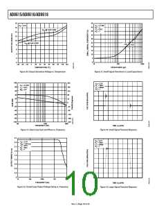
Figure 6. Input Offset Voltage Distribution
Figure 9. Input Bias Current vs. Temperature
22
20
18
16
14
12
10
8
1000
V
T
= ±2.5V
= –40°C TO +125°C
= 0V
S
V
T
= 5V
= 25°C
A
S
A
V
CM
100
10
SINK
SOURCE
6
1
4
2
0
0.1
0.001
0
2
4
6
8
10
12
100
0.01
0.1
I
1
10
(mA)
TCV
(μV/°C)
LOAD
OS
Figure 10. Output Voltage to Supply Rail vs. Load Current
Figure 7. Offset Voltage Drift Distribution
500
400
120
100
80
60
40
20
0
V
T
= 5V
= 25
S
A
V
= 5V
S
°C
300
10mA LOAD
200
100
0
–100
–200
–300
–400
–500
1mA LOAD
0
0.5
1.0
1.5
2.0
2.5
3.0
3.5
4.0
4.5
5.0
–40 –25 –10
5
20
35
50
65
C)
80
95 110 125
COMMON-MODE VOLTAGE (V)
TEMPERATURE (
°
Figure 8. Input Offset Voltage vs. Common-Mode Voltage
(200 Units, Five Wafer Lots Including Process Skews)
Figure 11. Output Saturation Voltage vs. Temperature
Rev. C | Page 6 of 20

 ADI [ ADI ]