AD8615/AD8616/AD8618
10
0
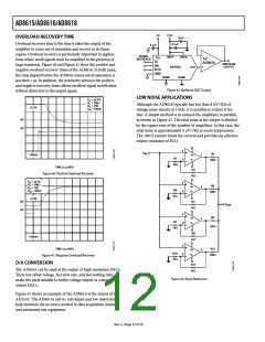
HIGH SPEED PHOTODIODE PREAMPLIFIER
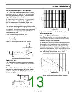
The AD8615/AD8616/AD8618 are excellent choices for I-to-V
conversions. The very low input bias, low current noise, and
high unity-gain bandwidth of the parts make them suitable,
especially for high speed photodiode preamps.
–10
–20
–30
–40
In high speed photodiode applications, the diode is operated
in a photoconductive mode (reverse biased). This lowers the
junction capacitance at the expense of an increase in the
amount of dark current that flows out of the diode.
The total input capacitance, C1, is the sum of the diode and op
amp input capacitances. This creates a feedback pole that causes
degradation of the phase margin, making the op amp unstable.
Therefore, it is necessary to use a capacitor in the feedback to
compensate for this pole.
0.1
1
10
100
1k
10k
100k
1M
FREQUENCY (Hz)
Figure 46. Second-Order Butterworth, Low-Pass Filter Frequency Response
POWER DISSIPATION
To get the maximum signal bandwidth, select
Although the AD8615/AD8616/AD8618 are capable of
providing load currents up to 150 mA, the usable output, load
current, and drive capability is limited to the maximum power
dissipation allowed by the device package.
C1
2πR2 fU
C2 =
where fU is the unity-gain bandwidth of the amplifier.
In any application, the absolute maximum junction temperature
for the AD8615/AD8616/AD8618 is 150°C. This should never
be exceeded because the device could suffer premature failure.
Accurately measuring power dissipation of an integrated circuit
is not always a straightforward exercise; Figure 47 is a design aid
for setting a safe output current drive level or selecting a heat
sink for the package options available on the AD8616.
C2
R2
+2.5V
–
V–
I
R
C
C
IN
D
SH
D
V+
1.5
+
–2.5V
–V
BIAS
Figure 44. High Speed Photodiode Preamplifier
1.0
SOIC
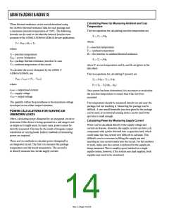
ACTIVE FILTERS
The low input-bias current and high unity-gain bandwidth
of the AD8616 make it an excellent choice for precision filter
design.
MSOP
0.5
Figure 45 shows the implementation of a second-order, low-
pass filter. The Butterworth response has a corner frequency
of 100 kHz and a phase shift of 90°. The frequency response
is shown in Figure 46.
0
0
20
40
60
80
100
120
140
TEMPERATURE (
°
C)
2nF
Figure 47. Maximum Power Dissipation vs. Ambient Temperature
V
CC
V–
V+
1.1kΩ
1.1kΩ
V
1nF
IN
V
EE
Figure 45. Second-Order, Low-Pass Filter
Rev. C | Page 13 of 20

 ADI [ ADI ]