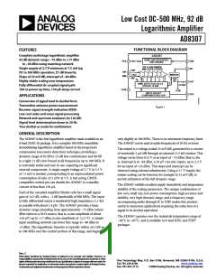
AD8307
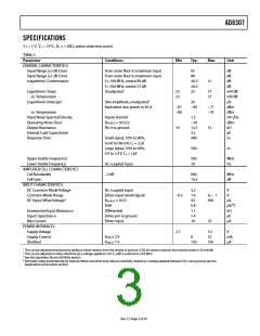
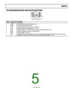
PIN CONFIGURATION AND FUNCTION DESCRIPTIONS
INP
INM
COM
OFS
OUT
1
2
3
4
8
7
6
5
VPS
ENB
INT
AD8307
TOP VIEW
(Not to Scale)
Figure 2. Pin Configuration
Table 3. Pin Function Descriptions
Pin No.
Mnemonic Description
±
2
3
4
5
6
7
8
INM
COM
OFS
OUT
INT
ENB
VPS
INP
Signal Input Minus Polarity. Normally at VPOS/2.
Common Pin (Usually Grounded).
Offset Adjustment. External capacitor connection.
Logarithmic (RSSI) Output Voltage. ROUT = ±2.5 kΩ.
Intercept Adjustment, ±3 dB (see the Slope and Intercept Adjustments section).
CMOS-Compatible Chip Enable. Active when high.
Positive Supply: 2.7 V to 5.5 V.
Signal Input Plus Polarity. Normally at VPOS/2. Due to the symmetrical nature of the response, there is no special
significance to the sign of the two input pins. DC resistance from INP to INM = ±.± kΩ.
Rev. C | Page 5 of 24

 ADI [ ADI ]