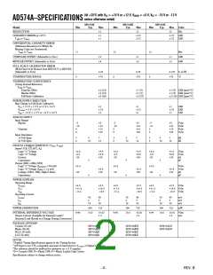
(@ +25؇C with VCC = +15 V or +12 V, VLOGIC = +5 V, VEE = –15 V or –12 V
AD574A–SPECIFICATIONS unless otherwise noted)
AD574AJ
Typ
AD574AK
Typ
AD574AL
Typ
Model
Min
11
0
Max
Min
12
0
Max
Min
12
0
Max
Units
RESOLUTION
12
12
12
Bits
LINEARITY ERROR @ +25°C
TMIN to TMAX
±1
±1
±1/2
±1/2
±1/2
±1/2
LSB
LSB
DIFFERENTIAL LINEARITY ERROR
(Minimum Resolution for Which No
Missing Codes are Guaranteed)
TMIN to TMAX
Bits
UNIPOLAR OFFSET (Adjustable to Zero)
BIPOLAR OFFSET (Adjustable to Zero)
±2
±4
±1
±4
±1
±2
LSB
LSB
FULL-SCALE CALIBRATION ERROR
(With Fixed 50 Ω Resistor from REF OUT to REF IN)
(Adjustable to Zero)
0.25
+70
0.25
+70
0.125 % of FS
+70 °C
TEMPERATURE RANGE
TEMPERATURE COEFFICIENTS
(Using Internal Reference)
T
MIN to TMAX
Unipolar Offset
Bipolar Offset
Full-Scale Calibration
±2 (10)
±2 (10)
±9 (50)
±1 (5)
±1 (5)
±5 (27)
±1 (5) LSB (ppm/°C)
±1 (5) LSB (ppm/°C)
±2 (10) LSB (ppm/°C)
POWER SUPPLY REJECTION
Max Change in Full-Scale Calibration
V
V
CC = 15 V ± 1.5 V or 12 V ± 0.6 V
LOGIC = 5 V ± 0.5 V
±2
±1/2
±2
±1
±1/2
±1
±1
±1/2
±1
LSB
LSB
LSB
VEE = –15 V ± 1.5 V or –12 V ± 0.6 V
ANALOG INPUT
Input Ranges
Bipolar
–5
–10
0
+5
–5
–10
0
+5
–5
–10
0
+5
Volts
Volts
Volts
Volts
+10
+10
+20
+10
+10
+20
+10
+10
+20
Unipolar
0
0
0
Input Impedance
10 Volt Span
20 Volt Span
3
6
5
10
7
14
3
6
5
10
7
14
3
6
5
10
7
14
kΩ
kΩ
DIGITAL CHARACTERISTICS1 (TMIN–TMAX
Inputs2 (CE, CS, R/C, A0)
Logic “1” Voltage
)
+2.0
–0.5
–20
+5.5
+0.8
+20
+2.0
–0.5
–20
+5.5
+0.8
+20
+2.0
–0.5
–20
+5.5
+0.8
+20
Volts
Volts
µA
Logic “0” Voltage
Current
Capacitance
5
5
5
5
5
5
pF
Output (DB11–DB0, STS)
Logic “1” Voltage (ISOURCE ≤ 500 µA)
Logic “0” Voltage (ISINK ≤ 1.6 mA)
Leakage (DB11–DB0, High-Z State)
Capacitance
+2.4
–20
+2.4
–20
+2.4
–20
Volts
Volts
µA
+0.4
+20
+0.4
+20
+0.4
+20
pF
POWER SUPPLIES
Operating Range
VLOGIC
+4.5
+5.5
+4.5
+5.5
+4.5
+5.5
Volts
VCC
VEE
+11.4
–11.4
+16.5
–16.5
+11.4
–11.4
+16.5
–16.5
+11.4
–11.4
+16.5 Volts
–16.5
Volts
Operating Current
ILOGIC
ICC
IEE
30
2
18
40
5
30
30
2
18
40
5
30
30
2
18
40
5
30
mA
mA
mA
POWER DISSIPATION
390
725
390
725
390
725
mW
INTERNAL REFERENCE VOLTAGE
9.98
10.0
10.02
1.5
9.98
10.0
10.02
1.5
9.99
10.0
10.01 Volts
1.5 mA
Output Current (Available for External Loads)3
(External Load Should not Change During Conversion)
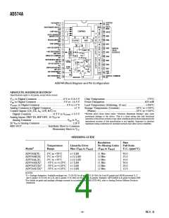
PACKAGE OPTIONS4
Ceramic (D-28)
Plastic (N-28)
PLCC (P-28A)
LCC (E-28A)
AD574ASD
AD574AJN
AD574AJP
AD574AJE
AD574AKD
AD574ALD
AD574ALN
AD574AKN
AD574AKP
AD574AKE
NOTES
1Detailed Timing Specifications appear in the Timing Section.
212/8 Input is not TTL-compatible and must be hard wired to VLOGIC or Digital Common.
3The reference should be buffered for operation on ±12 V supplies.
4D = Ceramic DIP; N = Plastic DIP; P = Plastic Leaded Chip Carrier.
Specifications subject to change without notice.
–2–
REV. B

 ADI [ ADI ]