AD574A
The full-scale trim is done by applying a signal 1 1/2 LSB below
the nominal full scale (9.9963 for a 10 V range). Trim R2 to
give the last transition (1111 1111 1110 to 1111 1111 1111).
START CONVERT
BIPOLAR OPERATION
STATUS
LOW IF CONVERSION
IN PROGRESS
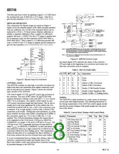
The connections for bipolar ranges are shown in Figure 5.
Again, as for the unipolar ranges, if the offset and gain specifica-
tions are sufficient, one or both of the trimmers shown can be
replaced by a 50 Ω ± 1% fixed resistor. Bipolar calibration is
similar to unipolar calibration. First, a signal 1/2 LSB above
negative full scale (–4.9988 V for the ±5 V range) is applied and
R1 is trimmed to give the first transition (0000 0000 0000 to
0000 0000 0001). Then a signal 1 1/2 LSB below positive full
scale (+4.9963 V the ±5 V range) is applied and R2 trimmed to
give the last transition (1111 11111110 to 1111 1111 1111).
CONVERT
R/C
CE
CS
VALUE OF A0
AT LAST CONVERT
COMMAND
A0
EOC8
READ
FROM
EOC12
NOTE 1
NIBBLE A, B,
ENABLE
12/8
(NOTE 2)
NIBBLE C
ENABLE
TO OUTPUT
BUFFERS
NIBBLE B = O
ENABLE
NOTE 1: WHEN START CONVERT GOES LOW, THE EOC (END OF CONVERSION) SIGNALS GO LOW.
EOC8 RETURNS HIGH AFTER AN 8-BIT CONVERSION CYCLE IS COMPLETE, AND EOC12
RETURNS HIGH WHEN ALL 12-BITS HAVE BEEN CONVERTED. THE EOC SIGNALS PREVENT
DATA FROM BEING READ DURING CONVERSIONS.
12/8
2
28
STS
3
4
5
CS
AO
27
24
HIGH
BIT
R/C
NOTE 2: 12/8 IS NOT A TTL-COMPATABLE INPUT AND SHOULD ALWAYS BE WIRED DIRECTLY TO
23
20
MIDDLE
BITS
VLOGIC OR DIGITAL COMMON.
6
CE
AD574A
R2
100Ω
19
16
LOW
BITS
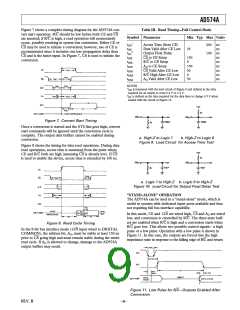
Figure 6. AD574A Control Logic
10
8
REF IN
GAIN
REF OUT
An output signal, STS, indicates the status of the converter.
STS goes high at the beginning of a conversion and returns low
when the conversion cycle is complete.
12 BIP OFF
OFFSET
R1
100Ω
1
+5V
+15V
–15V
Ϯ5V
ANALOG
13 10VIN
14 20VIN
7
INPUTS
11
Table I. AD574A Truth Table
Ϯ10V
15
DIG COM
ANA COM
9
CE CS R/C 12/8
AO Operation
0
X
X
1
X
X
X
X
X
X
None
None
Figure 5. Bipolar Input Connections
CONTROL LOGIC
The AD574A contains on-chip logic to provide conversion ini-
tiation and data read operations from signals commonly avail-
able in microprocessor systems. Figure 6 shows the internal
logic circuitry of the AD574A.
1
1
0
0
0
0
X
X
0
1
Initiate 12-Bit Conversion
Initiate 8-Bit Conversion
1
0
1
Pin 1
X
Enable 12-Bit Parallel Output
1
1
0
0
1
1
Pin 15 0
Pin 15 1
Enable 8 Most Significant Bits
Enable 4 LSBs + 4 Trailing Zeroes
The control signals CE, CS, and R/C control the operation of
the converter. The state of R/C when CE and CS are both
asserted determines whether a data read (R/C = 1) or a convert
(R/C = 0) is in progress. The register control inputs AO and
12/8 control conversion length and data format. The AO line is
usually tied to the least significant bit of the address bus. If a
conversion is started with AO low, a full 12-bit conversion cycle
is initiated. If AO is high during a convert start, a shorter 8-bit
conversion cycle results. During data read operations, AO deter-
mines whether the three-state buffers containing the 8 MSBs of
the conversion result (AO = 0) or the 4 LSBs (AO = 1) are
enabled. The 12/8 pin determines whether the output data is
to be organized as two 8-bit words (12/8 tied to DIGITAL
COMMON) or a single 12-bit word (12/8 tied to VLOGIC). The
12/8 pin is not TTL-compatible and must be hard-wired to
either VLOGIC or DIGITAL COMMON. In the 8-bit mode, the
byte addressed when AO is high contains the 4 LSBs from the
conversion followed by four trailing zeroes. This organization
allows the data lines to be overlapped for direct interface to
8-bit buses without the need for external three-state buffers.
TIMING
The AD574A is easily interfaced to a wide variety of micropro-
cessors and other digital systems. The following discussion of
the timing requirements of the AD574A control signals should
provide the system designer with useful insight into the opera-
tion of the device.
Table II. Convert Start Timing—Full Control Mode
Symbol Parameter
Min Typ Max Units
tDSC
tHEC
tSSC
tHSC
tSRC
tHRC
tSAC
tHAC
tC
STS Delay from CE
CE Pulse Width
CS to CE Setup
CS Low During CE High
R/C to CE Setup
400
ns
ns
ns
ns
ns
ns
ns
ns
300
300
200
250
R/C Low During CE High 200
AO to CE Setup
AO Valid During CE High
Conversion Time
8-Bit Cycle
0
300
It is not recommended that AO change state during a data read
operation. Asymmetrical enable and disable times of the
three-state buffers could cause internal bus contention resulting
in potential damage to the AD574A.
10
15
24
35
µs
µs
12-Bit Cycle
–8–
REV. B

 ADI [ ADI ]