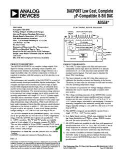
(@ TA = +25؇C, VCC = +5 V to +15 V unless otherwise noted)
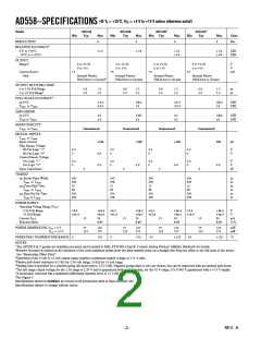
AD558–SPECIFICATIONS
Model
AD558J
Typ
AD558K
Typ
AD558S1
Typ
AD558T1
Typ
Min
Max
Min
Max
Min
Max
Min
Max
Units
RESOLUTION
8
8
8
8
Bits
RELATIVE ACCURACY2
0°C to +70°C
–55°C to +125°C
±1/2
±1/4
±1/2
±3/4
±1/4
±3/8
LSB
LSB
OUTPUT
Ranges3
0 to +2.56
0 to +10
0 to +2.56
0 to +10
0 to +2.56
0 to +10
0 to +2.56
0 to +10
V
V
Current Source
Sink
+5
+5
+5
+5
mA
Internal Passive
Internal Passive
Pull-Down to Ground
Internal Passive
Pull-Down to Ground
Internal Passive
Pull-Down to Ground
Pull-Down to Ground4
OUTPUT SETTLING TIME5
0 to 2.56 Volt Range
0.8
2.0
1.5
3.0
0.8
2.0
1.5
3.0
0.8
2.0
1.5
3.0
0.8
2.0
1.5
3.0
µs
µs
0 to 10 Volt Range4
FULL-SCALE ACCURACY6
@ 25°C
TMIN to TMAX
؎1.5
؎2.5
؎0.5
؎1
؎1.5
؎2.5
؎0.5
؎1
LSB
LSB
ZERO ERROR
@ 25°C
TMIN to TMAX
؎1
؎2
؎1/2
؎1
؎1
؎2
؎1/2
؎1
LSB
LSB
MONOTONICITY7
TMIN to TMAX
Guaranteed
Guaranteed
Guaranteed
Guaranteed
DIGITAL INPUTS
TMIN to TMAX
Input Current
±100
±100
±100
100
µA
Data Inputs, Voltage
Bit On-Logic “1”
Bit On-Logic “0”
Control Inputs, Voltage
On-Logic “1”
2.0
0
2.0
0
2.0
0
2.0
0
V
V
0.8
0.8
2.0
0
2.0
0
2.0
0
2.0
0
V
V
On-Logic “0”
0.8
0.8
0.8
Input Capacitance
4
4
4
4
pF
TIMING8
tW, Strobe Pulse Width
TMIN to TMAX
tDH Data Hold Time
TMIN to TMAX
tDS Data Set-Up Time
TMIN to TMAX
200
270
10
10
200
270
200
270
10
10
200
270
200
270
10
10
200
270
200
270
10
10
200
270
ns
ns
ns
ns
ns
ns
POWER SUPPLY
Operating Voltage Range (VCC
2.56 Volt Range
)
+4.5
+11.4
+16.5
+16.5
25
+4.5
+11.4
+16.5
+16.5
25
+4.5
+11.4
+16.5
+16.5
25
+4.5
+11.4
+16.5
+16.5
25
V
V
mA
%/%
10 Volt Range
Current (ICC
)
15
15
15
15
Rejection Ratio
0.03
0.03
0.03
0.03
POWER DISSIPATION, VCC = 5 V
VCC = 15 V
75
225
125
375
75
225
125
375
75
225
125
375
75
225
125
375
mW
mW
OPERATING TEMPERATURE RANGE
0
+70
0
+70
–55
+125
–55
+125
°C
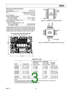
NOTES
1The AD558 S & T grades are available processed and screened lo MIL-STD-883 Class B. Consult Analog Devices’ Military Databook for details.
2Relative Accuracy is defined as the deviation of the code transition points from the ideal transfer point on a straight line from the offset to the full scale of the device.
See “Measuring Offset Error”.
3Operation of the 0 volt to 10 volt output range requires a minimum supply voltage of +11.4 volts.
4Passive pull-down resistance is 2 kΩ for 2.56 volt range, 10 kΩ for 10 volt range.
5Settling time is specified for a positive-going full-scale step to ±1/2 LSB. Negative-going steps to zero are slower, but can be improved with an external pull-down.
6The full range output voltage for the 2.56 range is 2.55 V and is guaranteed with a +5 V supply, for the 10 V range, it is 9.960 V guaranteed with a +15 V supply.
7A monotonic converter has a maximum differential linearity error of ±1 LSB.
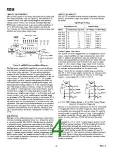
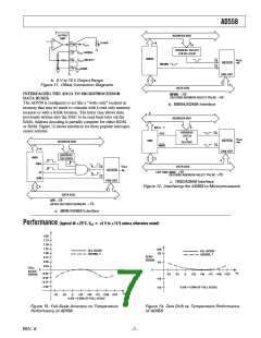
8See Figure 7.
Specifications shown in boldface are tested on all production units at final electrical test.
Specifications subject to change without notice.
–2–
REV. A

 ADI [ ADI ]