AD5399
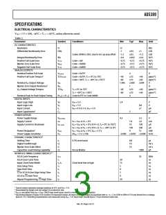
SPECIFICATIONS
ELECTRICAL CHARACTERISTICS
VDD = 5 V 1ꢀ0, –4ꢀ°C < TA < +1ꢀ5°C, unless otherwise noted.
Table 2.
Parameter
Symbol
Conditions
Min
Typ1
Max
Unit
DC CHARACTERISTICS
Resolution
N
12
Bits
Differential Nonlinearity Error
DNL
–1
0.5
0.5
0.02
–0.15
–0.15
–0.15
+1
LSB
LSB
%FS
%FS
%FS
%FS
Codes 2048 to 2052, due to int. op amp offset
–1.2
–0.4
–0.75
–0.75
–0.75
+1.2
+0.4
+0.75
+0.75
+0.75
Integral Nonlinearity Error
Positive Full-Scale Error
Bipolar Zero-Scale Error
Negative Full-Scale Error
ANALOG OUTPUTS
INL
V+FSE
VBZSE
V–FSE
Code = 0xF
Code = 0x000
Code = 0x800
Nominal Positive Full-Scale
Positive Full-Scale Tempco2
VOUTA/B
TCVOUTA/B
Code = 0x7FF
Code = 0x7FF, TA = 0°C to 70°C
Code = 0xFF, TA = –40°C to +105°C
4
V
–40
–60
1.995
10
10
2.000
1
+40
+60
2.004
ppm/°C
ppm/°C
V
Nominal VBZ Output Voltage
Bipolar Zero Output Resistance2
VBZ Output Voltage Tempco
VBZ
RBZ
Ω
TCVBZ
TA = 0°C to 70°C
TA = –40°C to +105°C
Code 0x7FF to Code 0x800
–40
–60
10
10
4
+40
+60
ppm/°C
ppm/°C
V
Nominal Peak-to-Peak Output Swing
DIGITAL INPUTS
|V+FS| + |V–FS|
Input Logic High
Input Logic Low
Input Current
Input Capacitance2
VIH
VIL
IIL
VDD = 5 V
VDD = 5 V
VIN = 0 V or 5 V, VDD = 5 V
2.4
4.5
V
V
µA
pF
0.8
1
CIL
5
POWER SUPPLIES
Power Supply Range
Supply Current
VDD RANGE
IDD
IDD_SHDN
5.5
2.6
100
500
13
V
VIH = VDD or VIL = 0 V
1.8
10
100
9
mA
µA
µA
mW
Supply Current in Shutdown
VIH = VDD or VIL = 0 V, B14 = 0, TA = 0°C to 105°C
VIH = VDD or VIL = 0 V, B14 = 0, TA = –40°C to 0°C
VIH = VDD or VIL = 0 V, VDD = 5.5 V
∆VDD = 5 V 10%
Power Dissipation3
PDISS
PSS
Power Supply Sensitivity
DYNAMIC CHARACTERISTICS2
Settling Time
–0.006 +0.003 +0.006 %/%
tS
Q
G
0.1% error band
No oscillation
0.8
10
10
µs
Digital Feedthrough
nV-s
nV-s
pF
Bipolar Zero-Scale Glitch
Capacitive Load Driving Capability
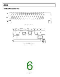
INTERFACE TIMING CHARACTERISTICS2, 4
SCLK Cycle Frequency
SCLK Clock Cycle Time
Input Clock Pulse Width
Data Setup Time
CL
1000
33
tCYC
t1
t2, t3
t4
MHz
ns
ns
30
15
5
Clock level low or high
ns
Data Hold Time
t5
0
ns
CS
to SCLK Active Edge Setup Time
CS
t6
5
ns
SCLK to Hold Time
t7
0
ns
CS
Repeat Programming, High Time
t8
30
ns
1 Typical values represent average readings at 25°C and VDD = 5 V.
2 Guaranteed by design and not subject to production test.
3 PDISS is calculated from (IDD × VDD). CMOS logic level inputs result in minimum power dissipation.
4 See timing diagram (Figure 5) for location of measured values. All input control voltages are specified with tR = tF = 2 ns (10% to 90% of 3 V) and timed from a voltage
level of 1.5 V. Switching characteristics are measured using VDD = 5 V. Input logic should have a 1 V/µs minimum slew rate.
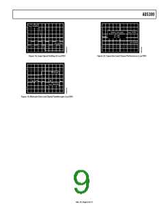
Rev. D | Page 3 of 12

 ADI [ ADI ]