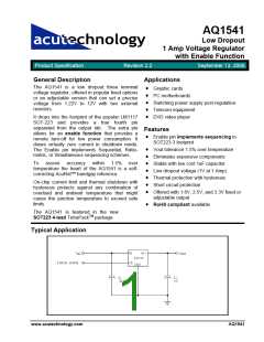
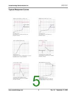
Acutechnology Semiconductor Inc.
AQ1541
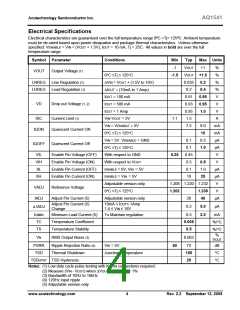
Electrical Specifications
Electrical characteristics are guaranteed over the full temperature range 0ºC <Tj< 125ºC. Ambient temperature
must be de-rated based upon power dissipation and package thermal characteristics. Unless otherwise
specified: VENABLE = VIN = (VOUT + 1.5V), IOUT = 10 mA, Tj = 25C. All values in bold are over the full
temperature range.
Symbol Parameter
Conditions
Min
Typ
Max Units
-1
VOUT
VOUT
0.035
0.2
+1
+1.5
0.2
%
%
%
%
V
VOUT
Output Voltage (1)
-1.5
0°C ≤Tj ≤ 125°C
LNREG
LDREG
Line Regulation (1)
Load Regulation (1)
∆VIN = VOUT + (1.5V to 10V)
∆IOUT = (10mA to 1 Amp)
IOUT = 100 mA
0.4
0.91
0.93
0.95
1.5
0.95
0.95
1.0
VD
Drop out Voltage (1, 2)
IOUT = 500 mA
V
IOUT = 1 Amp
V
ISC
Current Limit (1)
VIN-VOUT = 2V
1.1
A
VIN = VENABLE = 5V
0°C ≤Tj ≤ 125°C
7.5
9.0
10
mA
mA
µA
µA
V
IQON
Quiescent Current ON
VIN = 5V VENABLE = GND
0°C ≤Tj ≤ 125°C
0.1
0.1
0.45
0.5
0.1
10
0.5
1.0
IQOFF
Quiescent Current Off
VIL
VIH
IIL
Enable Pin Voltage (OFF)
Enable Pin Voltage (ON)
Enable Pin Current (OFF)
Enable Pin Current (ON)
With respect to GND
With respect to VOUT
ENABLE = 0V, VIN = 5V
ENABLE = VIN = 5V
Adjustable version only
0°C ≤Tj ≤ 125°C
0.25
0.8
1.0
25
V
µA
µA
V
IIH
1.208 1.220 1.232
VADJ
Reference Voltage
1.202
1.238
40
V
IADJ
Adjust Pin Current (5)
Adjustable version only
20
µA
Adjust Pin Current (5)
10mA ≤ IOUT≤ 1Amp
0.2
5.0
2.0
µA
∆ IADJ
Change
1.4 ≤ VIN ≤ 18V
IQMIN
TC
Minimum Load Current (5)
Temperature Coefficient
Temperature Stability
To Maintain regulation
0.5
0.005
0.5
mA
%/°C
%/°C
TS
%
VN
RMS Output Noise (3)
0.003
VOUT
PSRR
TSD
Ripple Rejection Ratio (4)
Thermal Shutdown
Vin = 5V
60
72
150
25
dB
°C
°C
Junction Temperature
TSDHYST TSD Hysteresis
Notes: (1) Low duty cycle pulse testing with Kelvin connections required.
(2) Measure (VIN - VOUT) when ∆VOUT, OR ∆VREF = 1%
(3) Bandwidth of 10Hz to 10kHz
(4) 120Hz input ripple
(5) Adjustable version only
www.acutechnology.com
4
Rev. 2.2 September 13, 2005

 ACUTECH [ ACUTECHNOLOGY SEMICONDUCTOR ]