ACT8810
Active- Semi
Rev 4, 01-Oct-09
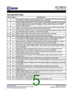
PIN DESCRIPTIONS CONT’D
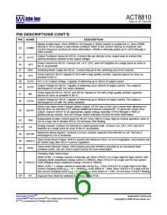
PIN NAME
DESCRIPTION
Master Enable Input. Drive nPBIN to GA through a 100kΩ resistor to enable the IC, drive nPBIN
directly to GA to assert a Hard-Reset condition. Refer to the System Startup & Shutdown and
Control Sequence sections for more information. nPBIN is internally pulled up to VSYS through a
50kΩ resistor.
24
25
nPBIN
OUT3
Output Feedback Sense for REG3. Connect this pin directly to the output node to connect the
internal feedback network to the output voltage.
Power Ground for REG3. Connect GA, GP1, GP2, and GP3 together at a single point as close to
the IC as possible.
26
27
28
29
30
GP3
SW3
VP3
Switching Node Output for REG3. Connect this pin to the switching end of the inductor.
Power Input for REG3. Bypass to GP3 with a high quality ceramic capacitor placed as close as
possible to the IC.
OUT6 RTC LDO Output Voltage. Capable of delivering up to 30mA of output current.
Output Voltage for REG5. Capable of delivering up to 360mA of output current. The output is
discharged to GA with 1kΩ when disabled.
OUT5
Power Input for REG4, REG5, and REG6. Bypass to GA with a high quality ceramic capacitor
placed as close as possible to the IC.
31
32
INL
Output Voltage for REG4. Capable of delivering up to 360mA of output current. The output is
discharged to GA with 1kΩ when disabled.
OUT4
Active-Low Open-Drain Charger Status Output. nSTAT has a 5mA (typ) current limit, allowing it to
directly drive an indicator LED without additional external components. To generate a logic-level
output, connect nSTAT to an appropriate supply voltage (typically VSYS) through a 10kΩ or
33
nSTAT
greater pull-up resistor. See the Charge Status Indication section for more information.
Independent Enable Control Input for REG2. Drive ON2 to a logic high for normal operation, drive to
GA or a logic low to disable REG2. Do not leave ON2 floating.
34
35, 37
36
ON2
Analog Ground. Connect GA directly to a quiet ground node. Connect GA, GP1, GP2, and GP3
together at a single point as close to the IC as possible.
GA
Reference Noise Bypass. Connect a 0.01μF ceramic capacitor from REFBP to GA. This pin is
discharged to GA in shutdown.
REFBP
Open-Drain Reset Output. nRSTO asserts low whenever REG1 is out of regulation, and remains low
for 260ms (typ) after REG1 reaches regulation.
38
nRSTO
Open-Drain Interrupt Output. nIRQ asserts any time nPBIN is asserted or an unmasked fault
condition exists. See the nIRQ Output section for more information.
39
nIRQ
Charging State Select Input.
When ACIN = 0 charge current is internally set; Drive CHGLEV to a logic-high for high-current USB
charging mode (maximum charge current is 500mA), drive CHGLEV to a logic-low for low-current
40 CHGLEV USB charging mode (maximum charge current is 100mA).
When ACIN = 1 charge current is externally set by RISET; Drive CHGLEV to a logic-high to for high-
current charging mode (ICHG = K × 1000/RISET (mA) where K = 640), drive CHGLEV to a logic-low for
low-current charging mode (ICHG = K × 500/RISET (mA) where K = 640). Do not leave CHGLEV floating.
EP
EP
Exposed Pad. Must be soldered to ground on the PCB.
Innovative PowerTM
- 6 -
www.active-semi.com
ActivePMUTM and ActivePathTM are trademarks of Active-Semi.
Copyright © 2009 Active-Semi, Inc.
I2CTM is a trademark of Philips Electronics.

 ACTIVE-SEMI [ ACTIVE-SEMI, INC ]