ACT8810
Active- Semi
Rev 4, 01-Oct-09
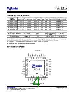
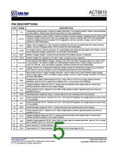
PIN DESCRIPTIONS
PIN NAME
DESCRIPTION
Temperature Sensing Input. Connect to battery thermistor. TH is pulled up with a 100µA current internally.
See the Battery Temperature Monitoring section for more information.
1
2
TH
Dynamic Charging Current Control. Connect a resistor to set the dynamic charging current control point.
A internal 100µA current source sets up a voltage that is used to compare with VSYS and dynamically
scale the charging current to maintain VSYS regulation. See the Dynamic Charge Current Control
section for more information.
DCCC
Safety Timer Program Pin. The resistance between this pin and GA determines the timers timeout
values. See the Charging Safety Timers section for more information.
3
4
BTR
AC Adaptor Detect. Detects presence of a wall adaptor and automatically adjusts the charge current
to the maximum charge current level. Do not leave ACIN floating.
ACIN
5, 6
7, 8
BAT
Battery Charger Output. Connect this pin directly to the battery anode (+ terminal)
System Output Pin. Bypass to GA with a 10µF or larger ceramic capacitor.
VSYS
Power Input for the Battery Charger. Bypass CHG_IN to GA with a capacitor placed as close to the
9
CHG_IN IC as possible. The battery charger are automatically enabled when a valid voltage is present on
CHG_IN. See the CHG_IN Bypass Capacitor Selection section for more information.
Charge Current Set. Program the maximum charge current by connecting a resistor (RISET) between
ISET and GA. See the Charger Current Programming section for more information.
10
11
ISET
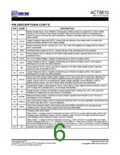
Step-Down DC/DCs Output Voltage Selection. Drive to logic low to select default output voltage.
Drive to logic high to select secondary output voltage. See the Output Voltage Selection Pin section
VSEL
for more information.
Independent Enable Control Input for REG1. Drive ON1 to VSYS or to a logic high for normal
operation, drive to GA or a logic low to disable REG1. Do not leave ON1 floating.
12
13
ON1
Output Feedback Sense for REG2. Connect this pin directly to the output node to connect the
internal feedback network to the output voltage.
OUT2
Power Input for REG2. Bypass to GP2 with a high quality ceramic capacitor placed as close as
possible to the IC.
14
15
16
VP2
SW2
GP2
Switching Node Output for REG2. Connect this pin to the switching end of the inductor.
Power Ground for REG2. Connect GA, GP1, GP2 and GP3 together at a single point as close to the
IC as possible.
Power Ground for REG1. Connect GA, GP1, GP2 and GP3 together at a single point as close to the
IC as possible.
17
18
19
GP1
SW1
VP1
Switching Node Output for REG1. Connect this pin to the switching end of the inductor.
Power Input for REG1. Bypass to GP1 with a high quality ceramic capacitor placed as close as
possible to the IC.
Output Feedback Sense for REG1. Connect this pin directly to the output node to connect the
internal feedback network to the output voltage.
20
21
OUT1
ON3
Enable Control Input for REG3. Drive ON3 to a logic high for normal operation, drive to GA or a logic
low to disable REG3. Do not leave ON3 floating.
22
23
SCL
SDA
Clock Input for I2C Serial Interface.
Data Input for I2C Serial Interface. Data is read on the rising edge of SCL.
Innovative PowerTM
- 5 -
www.active-semi.com
ActivePMUTM and ActivePathTM are trademarks of Active-Semi.
I2CTM is a trademark of Philips Electronics.
Copyright © 2009 Active-Semi, Inc.

 ACTIVE-SEMI [ ACTIVE-SEMI, INC ]