Actel Fusion Mixed-Signal FPGAs
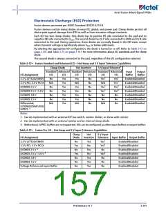
Electrostatic Discharge (ESD) Protection
Fusion devices are tested per JEDEC Standard JESD22-A114-B.
Fusion devices contain clamp diodes at every I/O, global, and power pad. Clamp diodes protect all
device pads against damage from ESD as well as from excessive voltage transients.
Each I/O has two clamp diodes. One diode has its positive (P) side connected to the pad and its
negative (N) side connected to VCCI. The second diode has its P side connected to GND and its N side
connected to the pad. During operation, these diodes are normally biased in the Off state, except
when transient voltage is significantly above VCCI or below GND levels.
By selecting the appropriate I/O configuration, the diode is turned on or off. Refer to Table 2-72 on
page 2-141 and Table 2-73 on page 2-141 for more information about I/O standards and the clamp
diode.
The second diode is always connected to the pad, regardless of the I/O configuration selected.
Table 2-72 • Fusion Standard and Advanced I/O – Hot-Swap and 5 V Input Tolerance Capabilities
Clamp Diode
Hot Insertion
5 V Input Tolerance1
Standard Advanced Standard Advanced Standard Advanced
Input
Buffer
Output
Buffer
I/O Assignment
3.3 V LVTTL/LVCMOS
3.3 V PCI, 3.3 V PCI-X
LVCMOS 2.5 V
I/O
No
N/A
No
No
No
No
N/A
I/O
Yes
Yes
Yes
Yes
Yes
Yes
Yes
I/O
Yes
N/A
Yes
Yes
Yes
Yes
N/A
I/O
No
No
No
No
No
No
No
I/O
Yes1
N/A
Yes1
Yes1
No
I/O
Yes1
Yes1
Yes2
Yes2
No
Enabled/Disabled
Enabled/Disabled
Enabled/Disabled
Enabled/Disabled
Enabled/Disabled
Enabled/Disabled
Enabled/Disabled
LVCMOS 2.5 V / 5.0 V
LVCMOS 1.8 V
LVCMOS 1.5 V
No
No
Differential,
N/A
No
LVDS/BLVDS/M-LVDS/
LVPECL 3
Notes:
1. Can be implemented with an external IDT bus switch, resistor divider, or Zener with resistor.
2. Can be implemented with an external resistor and an internal clamp diode.
3. Bidirectional LVPECL buffers are not supported. I/Os can be configured as either input buffers or output buffers.
Table 2-73 • Fusion Pro I/O – Hot-Swap and 5 V Input Tolerance Capabilities
Clamp
Diode
Hot
5 V Input
I/O Assignment
Insertion Tolerance Input Buffer Output Buffer
3.3 V LVTTL/LVCMOS
3.3 V PCI, 3.3 V PCI-X
LVCMOS 2.5 V 3
No
Yes
No
Yes
No
No
No
Yes
No
Yes1
Yes1
No
Enabled/Disabled
Enabled/Disabled
Enabled/Disabled
Enabled/Disabled
Enabled/Disabled
Enabled/Disabled
Enabled/Disabled
Yes
No
LVCMOS 2.5 V / 5.0 V 3
Yes2
LVCMOS 1.8 V
Yes
Yes
Yes
No
LVCMOS 1.5 V
No
Voltage-Referenced Input Buffer
No
Preliminary v1.7
2-141

 ACTEL [ Actel Corporation ]