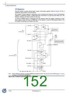
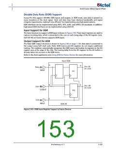
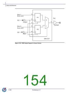
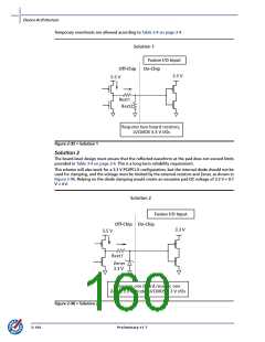
Device Architecture
For Fusion devices requiring Level 3 and/or Level 4 compliance, the board drivers connected to
Fusion I/Os need to have 10 kΩ (or lower) output drive resistance at hot insertion, and 1 kΩ (or
lower) output drive resistance at hot removal. This is the resistance of the transmitter sending a
signal to the Fusion I/O, and no additional resistance is needed on the board. If that cannot be
assured, three levels of staging can be used to meet Level 3 and/or Level 4 compliance. Cards with
two levels of staging should have the following sequence:
1. Grounds
2. Powers, I/Os, other pins
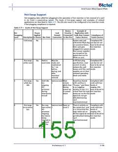
Cold-Sparing Support
Cold-sparing means that a subsystem with no power applied (usually a circuit board) is electrically
connected to the system that is in operation. This means that all input buffers of the subsystem
must present very high input impedance with no power applied so as not to disturb the operating
portion of the system.
Pro I/O banks and standard I/O banks fully support cold-sparing.
For Pro I/O banks, standards such as PCI that require I/O clamp diodes, can also achieve cold-sparing
compliance, since clamp diodes get disconnected internally when the supplies are at 0 V.
For Advanced I/O banks, since the I/O clamp diode is always active, cold-sparing can be
accomplished either by employing a bus switch to isolate the device I/Os from the rest of the system
or by driving each advanced I/O pin to 0 V.
If Standard I/O banks are used in applications requiring cold-sparing, a discharge path from the
power supply to ground should be provided. This can be done with a discharge resistor or a
switched resistor. This is necessary because the standard I/O buffers do not have built-in I/O clamp
diodes.
If a resistor is chosen, the resistor value must be calculated based on decoupling capacitance on a
given power supply on the board (this decoupling capacitor is in parallel with the resistor). The RC
time constant should ensure full discharge of supplies before cold-sparing functionality is required.
The resistor is necessary to ensure that the power pins are discharged to ground every time there is
an interruption of power to the device.
I/O cold-sparing may add additional current if the pin is configured with either a pull-up or pull
down resistor and driven in the opposite direction. A small static current is induced on each IO pin
when the pin is driven to a voltage opposite to the weak pull resistor. The current is equal to the
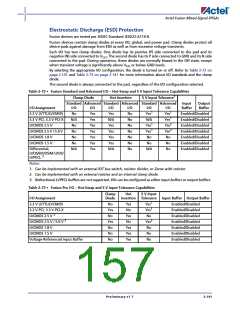
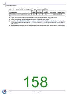
voltage drop across the input pin divided by the pull resistor. Please refer to Table 2-92 on
page 2-169, Table 2-93 on page 2-169, and Table 2-94 on page 2-171 for the specific pull resistor
value for the corresponding I/O standard.
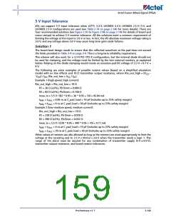
For example, assuming an LVTTL 3.3 V input pin is configured with a weak Pull-up resistor, a current
will flow through the pull-up resistor if the input pin is driven low. For an LVTTL 3.3 V, pull-up
resistor is ~45 kΩ and the resulting current is equal to 3.3 V / 45 kΩ = 73 µA for the I/O pin. This is
true also when a weak pull-down is chosen and the input pin is driven high. Avoiding this current
can be done by driving the input low when a weak pull-down resistor is used, and driving it high
when a weak pull-up resistor is used.
In Active and Static modes, this current draw can occur in the following cases:
•
•
•
•
•
•
•
•
Input buffers with pull-up, driven low
Input buffers with pull-down, driven high
Bidirectional buffers with pull-up, driven low
Bidirectional buffers with pull-down, driven high
Output buffers with pull-up, driven low
Output buffers with pull-down, driven high
Tristate buffers with pull-up, driven low
Tristate buffers with pull-down, driven high
2-140
Preliminary v1.7

 ACTEL [ Actel Corporation ]