0.27
A CURRENT CONSUMPTION VOLTAGE DETECTOR WITH DELAY FUNCTION (EXTERNAL DELAY TIME SETTING)
Rev.5.1_03
S-1009 Series
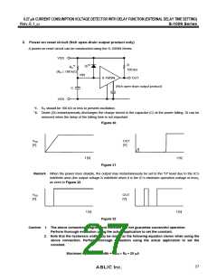
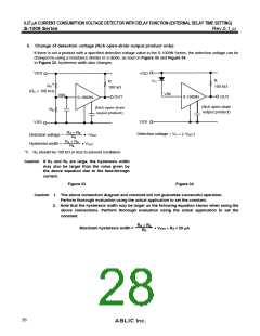
2. Power-on reset circuit (Nch open-drain output product only)
A power-on reset circuit can be constructed using the S-1009N Series.
VDD
Di*2
VIN
R
100 k
*1
RA
(RA 100 k)
S-1009N
OUT
(Nch open-drain output product)
C
VSS
*1. RA should be 100 k or less to prevent oscillation.
*2. Diode (Di) instantaneously discharges the charge stored in the capacitor (C) at the power falling. Di can be
removed when the delay of the falling time is not important.
Figure 30
VDD
[V]
OUT
[V]
t [s]
t [s]
Figure 31
Remark When the power rises sharply, the output may instantaneously be set to the "H" level due to the IC’s
indefinite area (the output voltage is indefinite when it is the IC’s minimum operation voltage or less),
as seen in Figure 32.
VDD
[V]
OUT
[V]
t [s]
t [s]
Figure 32
Caution 1. The above connection diagram and constant will not guarantee successful operation.
Perform thorough evaluation using the actual application to set the constant.
2. Note that the hysteresis width may be larger as the following equation shows when using the
above connection. Perform thorough evaluation using the actual application to set the
constant.
Maximum hysteresis width = VHYS RA 20 A
27

 ABLIC [ ABLIC ]