0.27
A CURRENT CONSUMPTION VOLTAGE DETECTOR WITH DELAY FUNCTION (EXTERNAL DELAY TIME SETTING)
S-1009 Series
Rev.5.1_03
1 s
1 s
*1
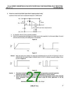
VIH
Input voltage
R*1
*2
VDD
100 k
VIL
VDD
tPHL
tPLH
OUT
CD
*1
V
VDD*3 90%
*3
VSS
VDD1
VDD
COUT
V
Output voltage
VDD*3 10%
*1. R and VDD1 are unnecessary for CMOS output
product.
*1. VIH = 10 V
*2. VIL = 0.7 V
*3. CMOS output product: VDD
Nch open-drain product: VDD1
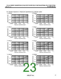
Figure 24 Test Condition of Response Time
Figure 25 Test Circuit of Response Time
Caution 1. The above connection diagram and constant will not guarantee successful operation.
Perform thorough evaluation using the actual application to set the constant.
2. When the CD pin is open, a double pulse may appear at release.
To avoid the double pulse, attach 100 pF or more capacitor to the CD pin.
Response time when detecting (tPHL) is not affected by CD pin capacitance. Besides, response
time when releasing (tPLH) can be set the delay time by attaching the CD pin.
Refer to "11. Delay time (tD) vs. CD pin capacitance (CD) (without output pin capacitance)" for
details.
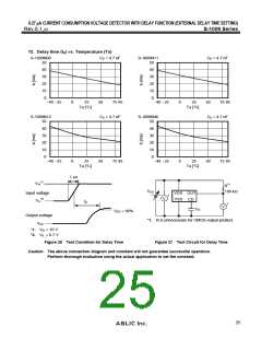
11. Delay time (tD) vs. CD pin capacitance (CD) (without output pin capacitance)
S-1009N08
10000
Ta = 25°C
S-1009N11
10000
Ta = 25°C
1000
100
10
1000
100
10
1
1
0.1
0.1
0.1
1
10
[nF]
100
1000
0.1
1
10
[nF]
100
1000
CD
CD
S-1009N12
10000
Ta = 25°C
S-1009N46
10000
Ta = 25°C
1000
100
10
1000
100
10
1
1
0.1
0.1
0.1
1
10
[nF]
100
1000
0.1
1
10
[nF]
100
1000
CD
CD
24

 ABLIC [ ABLIC ]