TP2121/TP2121N/TP2122/TP2124
1.8V, 600nA Nanopower, Rail-to-Rail Input/Output Op-amps
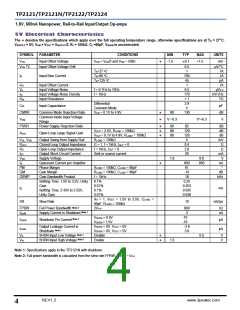
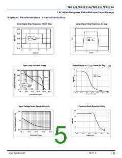
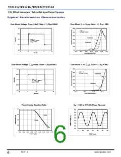
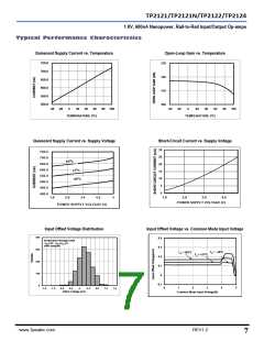
Typical Performance Characteristics
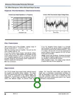
Closed-Loop Output Impedance vs. Frequency
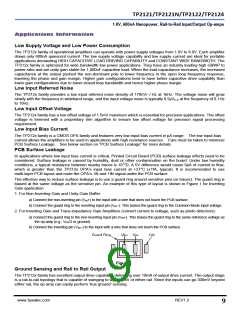
0.1Hz to 10Hz Time Domain Output Voltage Noise
5
4
100k
10k
1k
3
2
1
0
100
10
-1
-2
-3
-4
-5
1
1
10
100
1k
10k
-6
-4
-2
0
2
4
6
TIME (Seconds)
FREQUENCY (Hz)
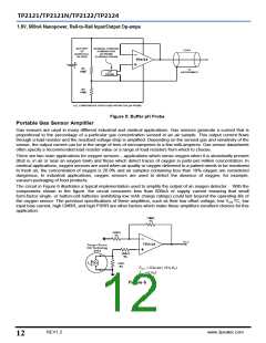
Pin Functions
–
–IN: Inverting Input of the Amplifier. Voltage range of
V– or VS: Negative Power Supply. It is normally
tied to ground. It can also be tied to a voltage other
than ground as long as the voltage between V+ and
V– is from 1.8V to 5.5V. If it is not connected to
ground, bypass it with a capacitor of 0.1μF as close
to the part as possible.
this pin can go from V– – 0.3V to V+ + 0.3V.
+IN: Non-Inverting Input of Amplifier. This pin has the
same voltage range as –IN.
V+ or +VS: Positive Power Supply. Typically the voltage
is from 1.8V to 5.5V. Split supplies are possible as long
as the voltage between V+ and V– is between 1.8V and
5.5V. A bypass capacitor of 0.1μF as close to the part as
possible should be used between power supply pins or
between supply pins and ground.
SHDN: Active Low Shutdown. Shutdown threshold
is 1.0V above negative supply rail. If unconnected,
the amplifier is automatically enabled.
OUT: Amplifier Output. The voltage range extends
to within milli-volts of each supply rail.
N/C: No Connection.
Operation
The TP212x family input signal range extends beyond
the negative and positive power supplies. The output
can even extend all the way to the negative supply. The
input stage is comprised of two CMOS differential
amplifiers, a PMOS stage and NMOS stage that are
active over different ranges of common mode input
voltage. The Class-AB control buffer and output bias
stage uses a proprietary compensation technique to
take full advantage of the process technology to drive
very high capacitive loads. This is evident from the
transient over shoot measurement plots in the Typical
Performance Characteristics.
REV1.2
www.3peakic.com
8

 3PEAK [ 3PEAK ]