TP2121/TP2121N/TP2122/TP2124
1.8V, 600nA Nanopower, Rail-to-Rail Input/Output Op-amps
The maximum output current is a function of total supply voltage. As the supply voltage to the amplifier increases, the
output current capability also increases. Attention must be paid to keep the junction temperature of the IC below 150°C
when the output is in continuous short-circuit. The output of the amplifier has reverse-biased ESD diodes connected to
each supply. The output should not be forced more than 0.5V beyond either supply, otherwise current will flow through
these diodes.
ESD
The TP212x family has reverse-biased ESD protection diodes on all inputs and output. Input and out pins can not be
biased more than 300mV beyond either supply rail.
Shut-down
The single channel OPA versions have SHDN pins that can shut down the amplifier to typical 3nA supply current. The
SHDN pin voltage needs to be within 0.5V of V– for the amplifier to shut down. During shutdown, the output will be in
high output resistance state, which is suitable for multiplexer applications. When left floating, the SHDN pin is internally
pulled up to the positive supply and the amplifier remains enabled.
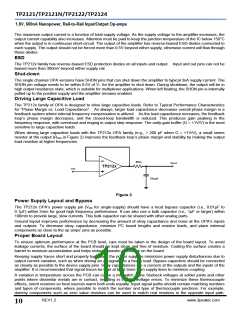
Driving Large Capacitive Load
The TP212x family of OPA is designed to drive large capacitive loads. Refer to Typical Performance Characteristics
for “Phase Margin vs. Load Capacitance”. As always, larger load capacitance decreases overall phase margin in a
feedback system where internal frequency compensation is utilized. As the load capacitance increases, the feedback
loop’s phase margin decreases, and the closed-loop bandwidth is reduced. This produces gain peaking in the
frequency response, with overshoot and ringing in output step response. The unity-gain buffer (G = +1V/V) is the most
sensitive to large capacitive loads.
When driving large capacitive loads with the TP212x OPA family (e.g., > 200 pF when G = +1V/V), a small series
resistor at the output (RISO in Figure 2) improves the feedback loop’s phase margin and stability by making the output
load resistive at higher frequencies.
Figure 2
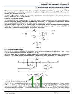
Power Supply Layout and Bypass
The TP212x OPA’s power supply pin (VDD for single-supply) should have a local bypass capacitor (i.e., 0.01μF to
0.1μF) within 2mm for good high frequency performance. It can also use a bulk capacitor (i.e., 1μF or larger) within
100mm to provide large, slow currents. This bulk capacitor can be shared with other analog parts.
Ground layout improves performance by decreasing the amount of stray capacitance and noise at the OPA’s inputs
and outputs. To decrease stray capacitance, minimize PC board lengths and resistor leads, and place external
components as close to the op amps’ pins as possible.
Proper Board Layout
To ensure optimum performance at the PCB level, care must be taken in the design of the board layout. To avoid
leakage currents, the surface of the board should be kept clean and free of moisture. Coating the surface creates a
barrier to moisture accumulation and helps reduce parasitic resistance on the board.
Keeping supply traces short and properly bypassing the power supplies minimizes power supply disturbances due to
output current variation, such as when driving an ac signal into a heavy load. Bypass capacitors should be connected
as closely as possible to the device supply pins. Stray capacitances are a concern at the outputs and the inputs of the
amplifier. It is recommended that signal traces be kept at least 5mm from supply lines to minimize coupling.
A variation in temperature across the PCB can cause a mismatch in the Seebeck voltages at solder joints and other
points where dissimilar metals are in contact, resulting in thermal voltage errors. To minimize these thermocouple
effects, orient resistors so heat sources warm both ends equally. Input signal paths should contain matching numbers
and types of components, where possible to match the number and type of thermocouple junctions. For example,
dummy components such as zero value resistors can be used to match real resistors in the opposite input path.
REV1.2
www.3peakic.com
10

 3PEAK [ 3PEAK ]