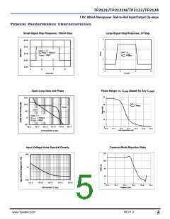
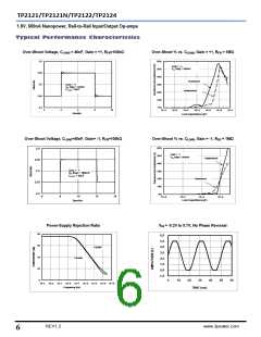
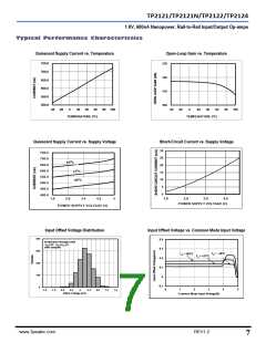
TP2121/TP2121N/TP2122/TP2124
1.8V, 600nA Nanopower, Rail-to-Rail Input/Output Op-amps
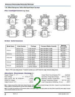
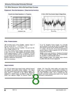
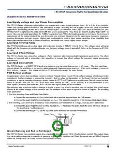
Pin Configuration(Top View)
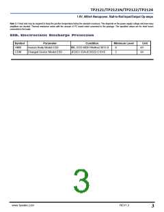
Order Information
Marking
Information
Model Name
Order Number
Package
Transport Media, Quantity
TP2121-TR
TP2121-CR
TP2121-SR
TP2121U-TR
TP2121N-TR
TP2121N-VR
TP2121N-SR
TP2122-SR
TP2122-VR
TP2124-SR
TP2124-TR
5-Pin SOT23
5-Pin SC70
8-Pin SOIC
5-Pin SOT23
6-Pin SOT23
8-Pin MSOP
8-Pin SOIC
8-Pin SOIC
8-Pin MSOP
14-Pin SOIC
14-Pin TSSOP
Tape and Reel, 3,000
Tape and Reel, 3,000
Tape and Reel, 4,000
Tape and Reel, 3,000
Tape and Reel, 3,000
Tape and Reel, 3,000
Tape and Reel, 4,000
Tape and Reel, 4,000
Tape and Reel, 3,000
Tape and Reel, 2,500
Tape and Reel, 3,000
B2TYW (1)
B2CYW (1)
2121S
B2UYW (1)
B2NYW (1)
2121N
TP2121
TP2121U
TP2121N
2121NS
B22S
TP2122
TP2124
B22V
B24S
B24T
Note (1): ‘YW’ is date coding scheme. 'Y' stands for calendar year, and 'W' stands for single workweek coding scheme.
Note 1
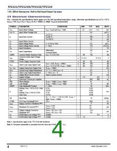
Absolute Maximum Ratings
Supply Voltage: V+ – V–....................................6.0V
Input Voltage............................. V– – 0.3 to V+ + 0.3
Input Current: +IN, –IN, SHDN Note 2.............. ±10mA
SHDN Pin Voltage……………………………V– to V+
Output Current: OUT.................................... ±20mA
Output Short-Circuit Duration Note 3…......... Indefinite
Operating Temperature Range.......–40°C to 125°C
Maximum Junction Temperature................... 150°C
Storage Temperature Range.......... –65°C to 150°C
Lead Temperature (Soldering, 10 sec) ......... 260°C
Note 1: Stresses beyond those listed under Absolute Maximum Ratings may cause permanent damage to the device. Exposure to any Absolute Maximum
Rating condition for extended periods may affect device reliability and lifetime.
Note 2: The inputs are protected by ESD protection diodes to each power supply. If the input extends more than 500mV beyond the power supply, the input
current should be limited to less than 10mA.
REV1.2
www.3peakic.com
2

 3PEAK [ 3PEAK ]