BRIGHT
Microelectronics
Inc.
BM29F400T/BM29F400B
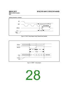
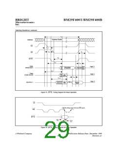
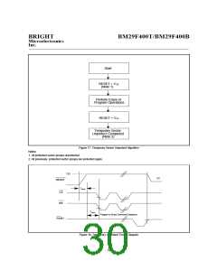
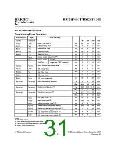
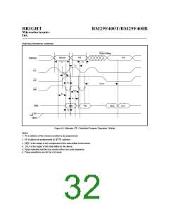
Switching Waveforms, continued
Data Polling
PA
PA
5555H
tWC
Address
CE
tAH
tAS
tGHWL
OE
tWP
tWHWH1
WE
tWPH
tCS
tD
Data
OUT
D
A0H
tDS
PD
DQ7
5.0V
Vcc
GND
Figure 19. Alternate
Controlled Program Operation Timings
CE
Notes:
1. PA is address of the memory location to be programmed.
2. PD is data to be programmed at address.
BYTE
is the output of the complement of the data written to the device.
3.
DQ7
4. DOUT is the output of the data written to the device.
5. Figure indicates last two bus cycles of four bus cycle sequence.
6. These waveforms are for the x16 mode.
- 32 -

 WINBOND [ WINBOND ]