BRIGHT
Microelectronics
Inc.
BM29F400T/BM29F400B
Switching Waveforms, continued
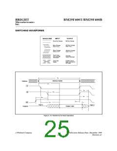
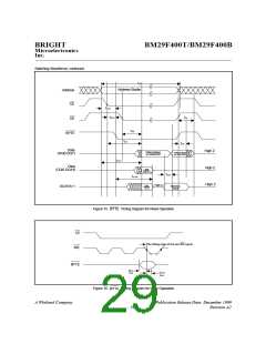
t
WC
Address Stable
Address
CE
t
AVFL
t
ELFL
t
DF
OE
t
OE
BYTE
t
CE
t
OH
Data
High Z
High Z
High Z
Data Output
on DQ0-DQ7
Data Output
on DQ0-DQ7
(DQ0-DQ7)
ACC
t
Data
(DQ8-DQ14)
Data
Outputon
DQ8-DQ14
t
ACC
t
FLQZ
Data
Outputon
DQ15
High Z
Address
Input
DQ15/A-1
Figure 15.
Timing Diagram for Read Operation
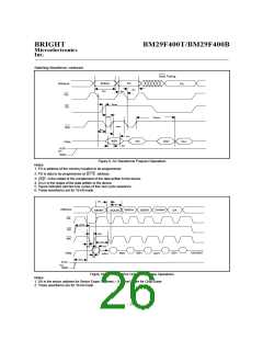
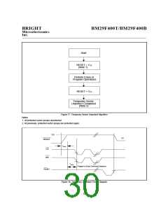
BYTE
CE
The falling edge of the last WE signal
WE
BYTE
tSET
(
)
tHOLD
tAS
(
)
tAH
Figure 16.
Timing Diagram for Write Operation
BYTE
A Winbond Company
Publication Release Date: December 1999
Revision A2
- 29 -

 WINBOND [ WINBOND ]