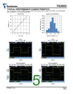
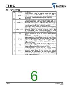
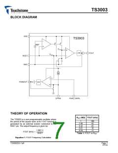
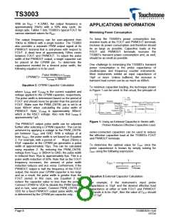
TS3003
ABSOLUTE MAXIMUM RATINGS
VDD to GND............................................................... -0.3V to +5.5V
PWM_CNTRLto GND .............................................. -0.3V to +5.5V
FOUT, PWMOUT to GND......................................... -0.3V to +5.5V
RSET to GND........................................................... -0.3V to +2.5V
CPWM to GND......................................................... -0.3V to +5.5V
FDIV to GND ............................................................ -0.3V to +5.5V
Continuous Power Dissipation (TA = +70°C)
10-Pin TDFN (Derate at 13.48mW/°C above +70°C)... 1078mW
Operating Temperature Range................................ -40°C to +85°C
Storage Temperature Range................................. -65°C to +150°C
Lead Temperature (Soldering, 10s).....................................+300°C
Electrical and thermal stresses beyond those listed under “Absolute Maximum Ratings” may cause permanent damage to the device. These
are stress ratings only and functional operation of the device at these or any other condition beyond those indicated in the operational sections
of the specifications is not implied. Exposure to any absolute maximum rating conditions for extended periods may affect device reliability and
lifetime.
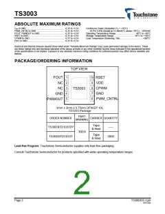
PACKAGE/ORDERING INFORMATION
PART
MARKING
ORDER NUMBER
TS3003ITD1033TP
TS3003ITD1033T
CARRIER QUANTITY
Tape
-----
& Reel
3003I
Tape
3000
& Reel
Lead-free Program: Touchstone Semiconductor supplies only lead-free packaging.
Consult Touchstone Semiconductor for products specified with wider operating temperature ranges.
Page 2
TS3003DS r1p0
RTFDS

 TOUCHSTONE [ TOUCHSTONE SEMICONDUCTOR INC ]