SMM465
Preliminary Information
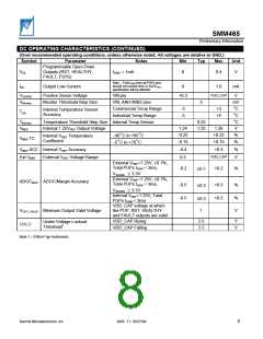
DC OPERATING CHARACTERISTICS (CONTINUED)
(Over recommended operating conditions, unless otherwise noted. All voltages are relative to GND.)
AIN1/AIN2 ADC characteristics
Symbol
Parameter
Notes
Min
Typ
Max
Unit
N
Resolution
10
Bits
Minimum resolution for which no
missing codes are guaranteed
MC
Missing Codes
10
Bits
S/N
DNL
INL
GAIN
Offset
Signal-to-Noise Ratio
Differential Non-Linearity
Integral Non-Linearity
Positive full scale gain error
Offset Error
Conversion rate = 500Hz
72
db
LSB
LSB
%
-1/2
-1
-0.5
-1
+1/2
+1
+0.5
+1
Note 1
Note 1
Note 1
LSB
Full Scale Temperature
ADC_TC
PPM/oC
±15
Coefficient
IMADC
IIVREF_ADC
Analog ADC Input Impedance
VREF_ADC Input Current
10
250
200
1
MΩ
nA
pF
ICVREF_ADC VREF_ADC Input Capacitance
IRVREF_ADC VREF_ADC Input Impedance
kΩ
Note 1 - The formula for the total ADC inaccuracy is: [((ADC read voltage) +/- INL)*(range of gain error)]+range of offset error
Summit Microelectronics, Inc
2085 1.1 05/27/04
9

 SUMMIT [ SUMMIT MICROELECTRONICS, INC. ]