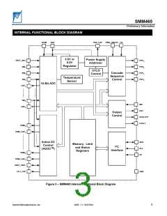
SMM465
Preliminary Information
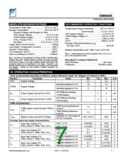
ABSOLUTE MAXIMUM RATINGS
RECOMMENDED OPERATING CONDITIONS
Temperature Under Bias....................... -55°C to 125°C
Storage Temperature............................ -65°C to 150°C
Terminal Voltage with Respect to GND:
Temperature Range (Industrial)...........–40°C to +85°C
(Commercial)............–5°C to +70°C
VDD Supply Voltage ..................................2.7V to 5.5V
12VIN Supply Voltage (1) ........................8.0V to 14.0V
VIN ............................................................ GND to VDD
VOUT...................................................... GND to 14.0V
Package Thermal Resistance (θJA)
VDD Supply Voltage ......................... -0.3V to 6.0V
12VIN Supply Voltage..................... -0.3V to 15.0V
PUPA, through PUPD....................... -0.3V to 15.0V
All Others ................................-0.3V to VDD + 0.7V
Output Short Circuit Current ............................... 100mA
Lead Solder Temperature (10 secs)....................300°C
Junction Temperature.......................…….....…...150°C
ESD Rating per JEDEC…………………....……..2000V
Latch-Up testing per JEDEC………..…....……±100mA
48 Lead TQFP……………………………….…80oC/W
Moisture Classification Level 1 (MSL 1) per J-STD- 020
Note 1 – Range depends on internal regulator set to 3.6V or 5.5V,
see 12VIN specification below.
Note - The device is not guaranteed to function outside its operating rating.
Stresses listed under Absolute Maximum Ratings may cause permanent
damage to the device. These are stress ratings only and functional operation
of the device at these or any other conditions outside those listed in the
operational sections of the specification is not implied. Exposure to any
absolute maximum rating for extended periods may affect device performance
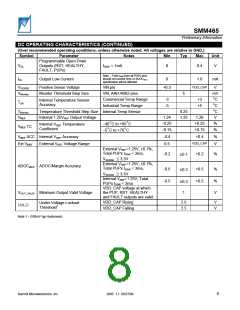
RELIABILITY CHARACTERISTICS
Data Retention…………………………..…..100 Years
Endurance…………………….……….100,000 Cycles
and reliability.
recommended.
Devices are ESD sensitive. Handling precautions are
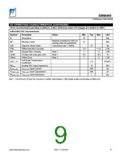
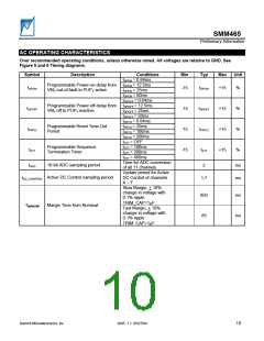
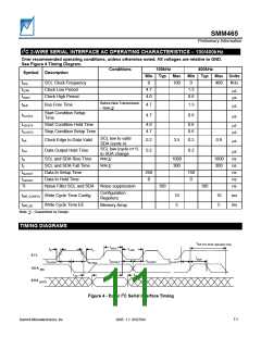
DC OPERATING CHARACTERISTICS
(Over recommended operating conditions, unless otherwise noted. All voltages are relative to GND.)
Symbol
Parameter
Supply Voltage
Notes
Min
2.7
10
Typ
Max
5.5
14
Unit
V
V
VDD
Internally regulated to 5.5V
Internally regulated to 3.6V
12VIN
Supply Voltage
6
14
V
All TRIM pins floating,
12VIN floating
All TRIM pins floating,
VDD floating
IDD
Power Supply Current from VDD
Power Supply Current from 12VIN
3
3
5
mA
I12VIN
5
mA
TRIM characteristics
TRIM Sourcing Maximum
1.5
mA
mA
V
TRIM output current through 100Ω to Current
ITRIM
1.0V
TRIM Sinking Maximum
1.5
Current
Depends on Trim range of
DC-DC Converter
VREF_CNTL/4
VTRIM
Margin Control and ADOC Range
VDD
All other input and output characteristics
VDD = 2.7V
VDD = 5.0V
VDD = 2.7V
VDD = 5.0V
Internally regulated to 3.6V
Internally regulated to 5.5V
Internally regulated to 3.6V
Internally regulated to 5.5V
0.9xVDD
0.7xVDD
-0.1
VDD
VDD
0.1xVDD
0.3xVDD
VDD
VDD
0.1xVDD
0.3xVDD
V
V
V
V
V
V
V
V
Input High Voltage (FS,
VIH
PWR_ON/OFF, MR#, SDA, SCL)
Input Low Voltage (FS,
VIL
PWR_ON/OFF, MR#, SDA, SCL)
-0.1
0.9xVDD
0.7xVDD
-0.1
Input High Voltage (FS,
VIH
PWR_ON/OFF, MR#, SDA, SCL)
Input Low Voltage (FS,
VIL
PWR_ON/OFF, MR#, SDA, SCL)
-0.1
Summit Microelectronics, Inc
2085 1.1 05/27/04
7

 SUMMIT [ SUMMIT MICROELECTRONICS, INC. ]