RT6263A/B
Electrical Characteristics
(VIN = 12V, TA = 25C, unless otherwise specified)
Parameter
Supply Voltage
Symbol
Test Conditions
Min Typ Max
Unit
VIN Supply Input Operating
Voltage
VIN
4.5
3.7
--
--
4
17
4.3
--
V
V
Under-Voltage Lockout
Threshold
VUVLO
Under-Voltage Lockout
Threshold Hysteresis
VUVLO
400
mV
Shutdown Current
Quiescent Current
Soft-Start
ISHDN
IQ
VEN = 0V
--
--
3
10
µA
µA
VEN = 2V, VFB = 0.8V
180
280
Soft-Start Internal Charging
Current
ISS
--
6
--
µA
Enable Voltage
VEN_H
VEN_L
EN high-level input voltage
EN low-level input voltage
1.16 1.25 1.34
Enable Voltage Threshold
V
1.01
225
1.1
1.19
900
EN Pin Pull-Down Resistance REN_DN
EN pin resistance to GND, V
= 12V
450
k
EN
Feedback Voltage and Discharge Resistance
Feedback Threshold Voltage VFB
V
= 1.05V
758
765
0
772
0.1
mV
OUT
Feedback Input Current
Internal MOSFET
IFB
V
FB
= 0.8V, T = 25°C
0.1
A
A
High-Side On-Resistance
Low-Side On-Resistance
Current Limit
RDS(ON)_H
RDS(ON)_L
VBOOT – VSW = 4.8V
--
--
66
36
--
--
mΩ
High-Side Switch Current
Limit
ILIM_H
ILIM_L
INOC
--
3.5
--
5.6
4.2
2.5
--
5.3
--
A
Low-Side Switch Valley
Current Limit
Low-Side Switch Negative
Current Limit
Forced PWM mode only
VOUT = 1.05V, PWM mode
A
Switching Frequency
Switching Frequency
On-Time Timer Control
On-Time
fSW
--
650
--
kHz
tON
VOUT = 1.05V
VFB = 0.5V
--
--
150
200
--
ns
ns
Minimum Off-Time
tOFF_MIN
260
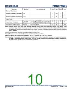
Output Under-Voltage Protections
UVP Trip Threshold
VUVP
Hiccup detect
--
--
--
65
1
--
--
--
%
Hiccup Power On-Time
Hiccup Power Off-Time
tHICCUP_ON Relative to SS time
tHICCUP_OFF Relative to SS time
cycle
cycles
7
Copyright © 2020 Richtek Technology Corporation. All rights reserved.
is a registered trademark of Richtek Technology Corporation.
DS6263A/B-00 January 2020
www.richtek.com
9

 RICHTEK [ RICHTEK TECHNOLOGY CORPORATION ]