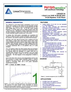
ADVANCE DATASHEET
14 Bit ADC
The LNDADC14 block is a very low current (typical 3.5uA in 14 bit
mode and 2.7uA in 10 bit mode) analog to digital converter
developed for low bandwidth battery operated portable electronics
applications. The LNDADC14 block uses the latest techniques in
low current data converter design. These newly derived techniques
obsolete many of the existing low current implementations with
respect to their power per conversion figure of merit (FOM). The
LNDADC14 block may be used independently or represents the
second stage cascade of the 18 Bit ΔΣ ADC block.
The LNDADC14 block operates from 2.7 to 3.6V Vin and
operates at a minimum 2.5kHz clock rate. The LNDADC14 block
features a user settable resolution from 8 to 14 bits to optimize
power savings (for example a signal may be sampled at 8 bits until it
meets certain criteria and then resolution improved to 14 bits to
improve feature accuracy at the price of more current for a period of
time).
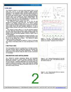
The LNDADC14 block utilizes a 1.5 bit self correcting quantizer
and fully differential internal analysis engine making it extremely
tolerant to noise, battery glitches, and comparator metastability. An
example of this self correcting capability is shown in Figure 3 (this is
an 8 bit example).
For extremely low current applications of limited bandwidth (<1uA)
the LNDADC14 block may be utilized in a wakeup and sleep mode
due to its fast startup time (<100us). The LNDADC14 utilizes
<100nA of current in sleep mode.
The LNDADC14 block features an ENOB of >12 bits in 14 bit mode
and >9 bits in 10 bit mode, an INL of +/-0.65 LSB and DNL of +/-0.45
LSB.
Figure 3 – Top Left: 1.5 bit quantizer of the 14 bit
pipeline ADC; Top Right: Self correcting operation of the
quantizer and; Bottom: Waveforms of the 14 bit ADC.
6 Bit Flash ADC
The 5 bit quantizer of the ΔΣ is created from a 6 bit flash converter.
The flash converter utilizes a differential delay line technique (see
Figure 4) to reduce tuning and silicon requirements. An accurate
transconductor and reference delay line allow accurate conversions
of >5 bit ENOB.
DECIMATION AND ANTIALIASING
The LNDADC18 includes antialiasing filtering and decimation
filtering with correction to ensure accurate conversion within the
signal band of interest. Figure 5 shows part of this filter in the form
of a sinc response. Additional digital filters and correction filters are
required to optimize the response. Figure 5 also shows the shuffling
DACs used to feedback the digitized information within the ΔΣ loop
and reduce tuning overhead.
Figure 4 – Left: Optimized transconductor for use with
differential delay line; Right: Partial differential delay line
with reference delay line.
Figure 5 – Left: Partial decimation filter sinc response;
Right: 32 element shuffling DAC.
Linear Dimensions Semiconductor Inc. 22620 Ricardo Rd, Cupertino CA 95014 USA tel 312.321.1810 fax 312.321.1830 www.lineardimensions.com

 RICHTEK [ RICHTEK TECHNOLOGY CORPORATION ]