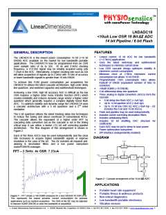
ADVANCE DATASHEET
LNDADC18
<10uA Low OSR 18 Bit ΔΣ ADC
14 bit Pipeline / 6 bit Flash
FEATURES
GENERAL DESCRIPTION
Lowest current 18 bit ADC for low bandwidth
(<=2.5kHz) applications
Uses the latest switchcap and subthreshold
techniques to minimize current draw
Low OSR cascade design optimizes stability &
minimizes current consumption
Minimum clock of 2.5kHz minimizes current
consumption but allows 16 bit ENOB
Programmable OSR (oversample rate) allows
tradeoff of ENOB (equivalent number of bits) to
resolution
The LNDADC18 is the lowest power consumption 18 bit (>16 bit
ENOB) ADC available on the market for low bandwidth portable
applications. The LNDADC18 may be programmed from an OSR
(over sample rate) of 4x to 32x. At 4x and 2.5kHz clocking
frequency, a 312.5Hz signal may be reliably acquired using only
7.23uA in the ADC. Alternatively, a higher clocking rate such as 32x
will allow acquisition of signals up to 2.5kHz with 16 bits of accuracy
or lower bandwidth signals to greater than 16 bits ENOB.
To achieve this FOM (power consumption per acquisition) the
LNDADC18 utilizes the latest cascade architecture, high order delay
line quantizer, and switched capacitor and subthreshold techniques.
>96dB SQNR (>16 ENOB)
5 bit differential delay line quantizer
Three analog to digital converters (ADCs) form the
cascade:
Achieving a low OSR, high bit accuracy ADC is difficult as the low
OSR requires a higher order noise transfer function (NTF) which
creates instability and reduces dynamic range and/or a higher order
quantizer which generally requires a complex digitally tuned flash
ADC. To optimize stability and dynamic range the LNDADC18 uses
a cascade architecture with a 5 bit quantizer and a 2nd order
modulator.
6 bit delay line flash ADC (<1uA typ)
Up to 14 bit pipeline ADC (<4uA typ)
Up to 18 bit low OSR ΔΣ ADC (<8uA typ – ΔΣ
includes the 6 bit and 14 bit ADCs)
Flash and pipeline may be used independently
Includes corner correcting decimation filters
Includes antialiasing filters
Includes 32 bit shuffling DAC structure for
coefficients
Each ADC may be put to sleep to save power
Power optimization subsystem
SPI Interface (independently enabled)
The 5 bit quantizer utilizes the latest tracking delay line techniques
to reduce the tuning and silicon overhead of conventional ADCs.
The cascade allows the equivalent of a higher order NTF by
cascading data converters but as the cascade is not in the timing
critical loop it can utilize a twelve (12) bit self correcting pipeline
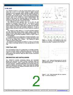
architecture. The flow diagram of this arrangement is shown in
Figure 2.
Each of the three ADCs may be used independently and the clock
rate increased to acquire higher bandwidth signals or improve
resolution in the case of the ΔΣ. The ΔΣ includes all required anti-
DIAGRAM
aliasing
& decimation filters and a low power subsystem
(nanoPOWER) manager.
FFT – 2.5kHz, 4x OSR, 7.23uA
Figure 2 – Cascade arrangement of the 18 bit ΔΣ ADC
APPLICATIONS
Portable heart rate equipment
Portable fitness & wellness products
Non-critical diagnostics
Low bandwidth portable electronics
Vibration sensors
Figure 1 – FFT shows a >96 SQNR sinewave for a low LNDADC18 OSR of 4x.
This represents the lowest possible current consumption for portable
applications such as medical acquisition. The OSR of the ΔΣ may be adjusted
to improve SQNR (ENOB) or raise the bandwidth of acquisition.
Linear Dimensions Semiconductor Inc. 22620 Ricardo Rd, Cupertino CA 95014 USA tel 312.321.1810 fax 312.321.1830 www.lineardimensions.com

 RICHTEK [ RICHTEK TECHNOLOGY CORPORATION ]