FM24CL16B - 16Kb 3V I2C F-RAM
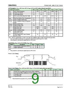
AC Parameters (TA = -40° C to + 85° C, VDD =2.7V to 3.65V unless otherwise specified)
Symbol Parameter Min Max Min Max Min Max Units Notes
fSCL
tLOW
tHIGH
tAA
SCL Clock Frequency
0
4.7
4.0
100
0
1.3
0.6
400
0
0.6
0.4
1000
kHz
1
Clock Low Period
µs
Clock High Period
SCL Low to SDA Data Out Valid
µs
µs
3
0.9
0.55
tBUF
Bus Free Before New Transmission
Start Condition Hold Time
Start Condition Setup for Repeated
Start
4.7
4.0
4.7
1.3
0.6
0.6
0.5
0.25
0.25
µs
µs
µs
tHD:STA
tSU:STA
tHD:DAT
tSU:DAT
tR
Data In Hold Time
0
250
0
100
0
100
ns
ns
ns
ns
µs
ns
Data In Setup Time
Input Rise Time
1000
300
300
300
300
100
2
2
tF
Input Fall Time
tSU:STO
Stop Condition Setup
Data Output Hold
4.0
0
0.6
0
0.25
0
tDH
(from SCL @ VIL)
tSP
Noise Suppression Time Constant
on SCL, SDA
50
50
50
ns
Notes : All SCL specifications as well as start and stop conditions apply to both read and write operations.
1
2
The speed-related specifications are guaranteed characteristic points from DC to 1 MHz.
This parameter is periodically sampled and not 100% tested.
Capacitance (TA = 25° C, f=1.0 MHz, VDD = 3V)
Symbol
CI/O
Parameter
Input/Output Capacitance (SDA)
Input Capacitance
Max
8
6
Units Notes
pF
pF
1
1
CIN
Notes
This parameter is periodically sampled and not 100% tested.
1
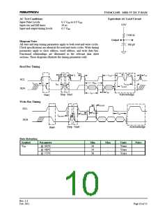
Power Cycle Timing
Power Cycle Timing (TA = -40°C to +85°C, VDD = 2.7V to 3.65V unless otherwise specified)
Symbol Parameter
Min
Max
Units
ms
Notes
tPU
Power Up (VDD min) to First Access (Start condition)
10
-
-
-
-
tPD
Last Access (Stop condition) to Power Down (VDD min)
0
µs
tVR
tVF
VDD Rise Time
VDD Fall Time
30
100
µ
s/V
s/V
1
1
µ
Notes
1. Slope measured at any point on VDD waveform.
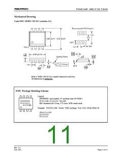
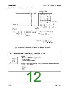
Rev. 1.4
Feb. 2011
Page 9 of 13

 RAMTRON [ RAMTRON INTERNATIONAL CORPORATION ]