FM22L16
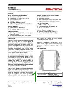
Figure 1. Block Diagram
Pin Description
Pin Name
Type Pin Description
A(17:0)
Input
Address inputs: The 18 address lines select one of 262,144 words in the FRAM array.
The lowest two address lines A(1:0) may be used for page mode read and write
operations.
/CE
Input
Chip Enable input: The device is selected and a new memory access begins when /CE is
low and /ZZ is high. The entire address is latched internally on the falling edge of /CE.
Subsequent changes to the A(1:0) address inputs allow page mode operation when /CE
is low.
/WE
Input
Write Enable: A write cycle begins when /WE is asserted. The rising edge causes the
FM22L16 to write the data on the DQ bus to the FRAM array. The falling edge of /WE
latches a new column address for fast page mode write cycles.
Output Enable: When /OE is low, the FM22L16 drives the data bus when valid read
data is available. De-asserting /OE high tri-states the DQ pins.
Sleep: When /ZZ is low, the device enters a low power sleep mode for the lowest
current condition. Since this input is logically AND’d with /CE, /ZZ must be high for
normal read/write operation.
/OE
/ZZ
Input
Input
DQ(15:0)
/UB
I/O
Input
Data: 16-bit bi-directional data bus for accessing the FRAM array.
Upper Byte Select: Enables DQ(15:8) pins during reads and writes. These pins are hi-Z
if /UB is high.
/LB
Input
Lower Byte Select: Enables DQ(7:0) pins during reads and writes. These pins are hi-Z
if /LB is high.
VDD
VSS
Supply Supply Voltage: 3.3V
Supply Ground
Rev. 1.0
Mar. 2007
Page 2 of 15

 RAMTRON [ RAMTRON INTERNATIONAL CORPORATION ]