OXCB950
OXFORD SEMICONDUCTOR LTD.
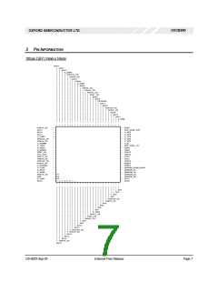
4 PIN DESCRIPTIONS
2
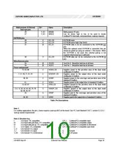
Cardbus/PCI bus Pins
Dir
Name
Description
1, 3, 4, 5, 8, 9, 10, 11, 16, 17, 18, C/P_I/O
19, 22, 23, 24, 25, 52, 53, 54, 57,
58, 60, 61, 66, 69, 73, 74, 75, 77,
78, 79, 100
AD[31:0]
Multiplexed Address/Data bus.
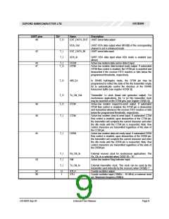
67, 80, 99, 15
C/P_I
C/BE[3:0]#
Multiplexed Command/Byte enable.
System clock
88
83
93
84
85
95
98
72
96
68
CP_I
CLK
1
CP_I
FRAME#
DEVSEL#
IRDY#
TRDY#
STOP#
PAR
Cycle Frame .
CP_O
CP_I
Device Select
Initiator ready
Target ready
CP_O
CP_O
CP_I/O
CP_O
CP_I/O
CP_I
Target Stop request
Parity
SERR#
PERR#
IDSEL
System error
Parity error
Initialisation device select
For PCI applications this pin must be connected to the IDSEL
pin on the PCI connector. For cardbus applications, there is
no IDSEL signal, so this pin must be tied to Vdd (3.3v) via a
pull-up on the board. (10K recommended).
86
94
59
CP_I
RST#
System reset
CP_OD
CP_O
INTA# /CINT#
CSYSCHG
Interrupt Pin. For both cardbus and pci applications
Power management event signal, for Cardbus applications
This pin must be No-Connect (NC) for PCI applications.
Power management event signal, for PCI applications
This pin must be No-Connect (NC) for cardbus applications.
Slew rate control for cardbus/pci outputs
51
32
CP_OD
I
PME#
SLEW_RATE
For cardbus applications, this must be tied to Vdd on the
board. For PCI applications, this must be tied to Gnd on the
board.
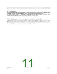
DS-0033 Sep 05
External-Free Release
Page 8

 OXFORD [ OXFORD SEMICONDUCTOR ]