OXCB950
OXFORD SEMICONDUCTOR LTD.
capabilities for Power Management and supporting the power states D0, D2 and D3. This achieves significant power savings by
allowing device drivers to power down the cardbus/PCI function and disable the UART channel.
A ‘wake-up’ event (the ‘power management event’) is requested via the PME# (PCI) or CSYSCHG (cardbus) pins from either of
the power states D2 or D3, by the UART line RI (for power state D3), and any modem line and the Serial Data In (for power state
D2).
Optional EEPROM:
TM
The OXCB950 can be reconfigured from an external Microwire based EEPROM. However, this is not required in many
applications as default values are provided for typical applications. Features available via the use of the EEPROM include
redefining device ID’s and vendor/sub-vendor ID fields in the PCI header space, cardbus-to-pci mode change, redefining Tuple
Information (relevant to cardbus applications only), and selectively enabling/disabling interrupts, powerdown and wakeup
requests.
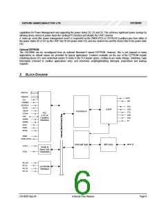
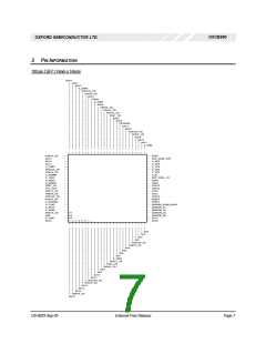
2 BLOCK DIAGRAM
AD[31:0]
C/BE[3:0]
SOUT
CLK
SIN
FRAME#
DEVSEL#
RTS
IRDY#
DTR
UART
TRDY#
Function 0
CTS
PCI
STOP#
DSR
3.3V or
PAR
CardBus
DCD
SERR#
Interface
RI
PERR#
RST#
IDSEL
INTA#
PME#
SLEW_RATE
MIO[1:0]
Interrupt logic
MIO pins
XTALO
XTALI
Clock &
Baud rate
Generator
EE_DO
EE_DI
EEPROM
interface
EE_CK
EE_CS
DS-0033 Sep 05
External-Free Release
Page 6

 OXFORD [ OXFORD SEMICONDUCTOR ]