Page No. : 3/13
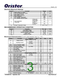
Absolute Maximum Ratings
Symbol
Parameter
Supply voltage Pin Voltage
VDD OVP maximal enter current
Input Voltage to FB Pin
Input Voltage to SEN Pin
Power Dissipation
ESD Capability, HBM Model
ESD Capability, Machine Model
Rating
40
20
-0.3 to 6V
-0.3 to 6V
300
Unit
V
mA
V
V
mW
V
VDD
IOVP
VFB
VSEN
PD
2500
250
ESD
V
20second:
SOT-23-6L
10second:
DIP-8
10second:
SOP-8
℃
220
260
Lead Temperature
(Soldering)
TL
℃
℃
230
TSTG
Storage Temperature Range
-55 to + 150
RECOMMENDED OPERATION CONDITION
Symbol
VDD
RI
TOA
PO
Parameter
VDD Supply Voltage
RI PIN Resistor Value
Min ~ Max
11~20
65~130
-20~85
0~80
Unit
V
K ohm
℃
Operation Ambient Temperature
Output Power
W
FPWM
Frequency of PWM
30~150
KHz
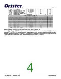
Electrical Characteristics (Ta=25°C unless otherwise noted, VDD = 15V.)
Symbol
Parameter
Conditions
Min.
Typ.
Max.
Unit
Supply Voltage (VDD Pin)
IST
Startup Current
1.5
3.2
2.2
1.65
12.8
7.8
μA
mA
mA
mA
V
VFB=0V
VFB=3V
VFB=Open
ISS
Operating Current
VDDON
Turn-on Threshold Voltage
VDDOFF Turn-off Threshold Voltage
VDCLAMP VDD Clamp Voltage
V
V
IVDD=20mA
25.6
Anti Intermission Surge
VDD Voltage
VDDAIS
12.7
V
TSS
TOFF
TRESTART
Soft start Time
Over temperature Protection
Temperature restart
1.2
130
100
mS
℃
℃
Voltage Feedback (FB Pin)
IFB
VFB
Short Circuit Current
Open Loop Voltage
VFB=0V
VFB=Open
1.57
4.6
mA
V
IFB_0D
IPFM
ICRM
VPFM
VCRM
Zero Duty Cycle FB current
1.47
1.37
1.45
0.51
0.30
152
4.2
mA
mA
mA
V
V
uA
V
Enter PFM&PWM, FB current
Enter CRM, FB current
PFM Threshold VFB
Enter CRM Threshold VFB
IOLP&SCP Enter OLP&SCP FB current
VOLP&SCP Enter OLP&SCP FB voltage
TOLP&SCP OLP&SCP min. delay Time
RI=100K
33
50
mS
Current Sensing (SEN Pin)
VTH_L
VTH_H
TPD
RCS
VSCP
TSCP
Minimum Voltage Lever
Maximum Voltage Lever
Delay to Output
Input Impedance
Sense short protect voltage
0.65
0.85
150
50
177
1.2
V
V
ns
KΩ
mV
mS
Sen. short protect Delay Time
Oscillator (RI Pin)
FOSC
Normal Frequency
RI=100Kohm
55
60
65
KHz
DS-RS2051-02
September, 2007
www.Orister.com

 ORISTER [ ORISTER CORPORATION ]