AMIS-52150 Low-Power Transceiver with Clock and Data Recovery
Data Sheet
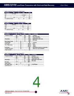
Table 9: Package Dimensions: 209mil SSOP
Inches
Millimeters
Max.
Dm
A
A1
A2
b
D
E
E1
e
Min.
0.068
0.002
0.065
0.009
0.271
0.291
0.197
Max.
0.078
.20
Min.
1.73
0.05
2.00
0.073
0.015
0.295
0.323
0.221
1.65`
0.22
6.90
7.40
5.00
1.85
0.38
7.5
0.820
0.560
0.026 BSC
0.65 BSC
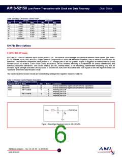
8.0 Pin Descriptions
8.1 RX1, RX2, RF Inputs
RX1 and RX2 are RF antenna inputs to the AMIS-52150. The internal circuit designs are identical between these inputs. The AMIS-
52150 receiver inputs, RX1 and RX2, require external components to match the low noise amplifier (LNA) to external devices such as
antennas. The external components must provide a DC voltage path to the RF ground. Figure 3 suggests an external circuit for the
receiver inputs at 403MHz. Each circuit’s input impedance can be trimmed internally to compensate for device manufacture and
external component tolerances. The circuits employ an LNA, internal filters, a low frequency, intermediate frequency (IF), and an
received signal strength indication (RSSI) circuit to recover the ASK/OOK modulated data. The signals in the two input channels are
“summed” before the data recovery circuit.
The functions of the receive circuits are controlled by writing to the registers shown in Table 10.
Table 10: Receiver Control Register Description
RX1 or RX2 Receiver Register Control
Register (HEX) Name
Bits
All
All
0
States
Comments
0x00
0x01
0x0c
ANT1 Trim
ANT2 Trim
ANT1 Enable
Inverse relationship register value to internal capacitance
Inverse relationship register value to internal capacitance
Antenna port is off
Antenna port is on
Antenna port is off
0
1
0
1
ANT2 Enable
1
Antenna port is on
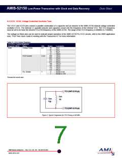
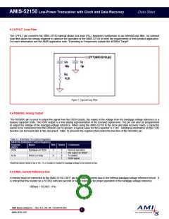
Figure 3: Typical Input Impedance Match to 50Ω (402MHz)
AMI Semiconductor – Rev 4.0, Oct. 06 – M-20535-004
6
www.amis.com

 ONSEMI [ ONSEMI ]