FEDL87V2107-01
OKI Semiconductor
ML87V2107
2.2.5 Input/Output Phase Difference Read
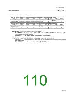
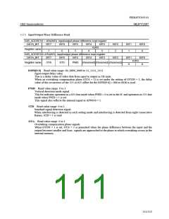
SUB_ADDRESS = 46h(W/R): Input/output phase difference read register
DATA_BIT
BIT7
BIT6
BIT5
BIT4
BIT3
BIT2
2
BIT1
BIT0
0
IOPD
Register name
7
6
5
4
3
1
BIT1
9
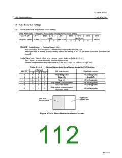
SUB_ADDRESS=47h(W/R): Input/output phase difference read register
DATA_BIT
BIT7
BIT6
BIT5
BIT4
BIT3
BIT2
BIT0
8
IOPD
Register name
OTA
STD
PNID
(Reserved) (Reserved) (Reserved)
IOPD[9:0] Read value range: 00_0000_0000 to 11_1111_1111
Input-output delay value.
This is a delay value of video data from input to output in 1H units.
When an overtaking compensation phase (OTA = 1) is set under the setting of OTON = 1, the delay
value of the occurrence of the 525 or 625 offset for the IOPD[9:0] = 000 to 002h is read.
PNID Read value range: 0 to 1
Vertical direction mode signal.
This bit indicates operation in a 625-line mode when PNID = 0 is set in the IC and operation in 525-line
mode when PNID = 1 is set.
This signal also reflects the internal signal at APN656 = 1.
STD Read value range: 0 to 1
Standard signal detection signal.
When interleaving is detected in each setting mode and interleaving is detected from eight consecutive
frames, STD = 1 is read.
OTA Read value range: 0 to 1
Overtaking compensation phase signals.
When OTON = 1 is set, OTA = 1 is generated when the phase difference between the input and the
output becomes smaller and Sync. signals are approached to the phase in which overtaking occurs in the
internal memory.
111/152

 OKI [ OKI ELECTRONIC COMPONETS ]