FEDL87V2107-01
OKI Semiconductor
ML87V2107
2. Description of the Registers
2.1 Mode Setting
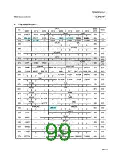
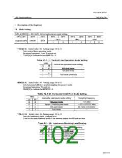
SUB_ADDRESS = 40h (W/R): Write/read common mode setting
DATA_BIT
BIT7
BIT6
BIT5
BIT4
BIT3
1
BIT2
0
BIT1
1
BIT0
YBLS
HMD
VMD
0
Register name IRMON
R601
1
0
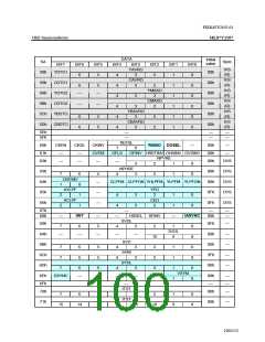
VMD[1:0] Initial value: 00; Setting range: 00 to 11
Sets vertical lines operation mode.
In normal operation, 2 and 3 are not set.
VMD[0] is validated when IRMON = 1.
Table R2-1 (1) Vertical Line Operation Mode Setting
VMD
Vertical line operation mode setting
[1]
0
[0]
0
625-line mode
0
1
525-line mode
1
0
Test mode (79 lines)
1
1
HMD[1:0] Initial value: 00; Setting range: 00 to 11
Sets horizontal effective pixels (sampling frequency) mode.
In normal operation, 3 is not set.
HMD[0] is validated at IRMON = 1.
Table R2-1 (2) Horizontal Valid Pixel Mode Setting
HMD
[1]
Horizontal valid pixels mode setting
Sampling frequency
[0]
0
0
0
1
1
720-pixel mode
Square (768/640) pixel mode
768-pixel mode
13.5 MHz
14.75/12.272727 MHz
14.75/14.31818 MHz
—
1
0
1
Test mode
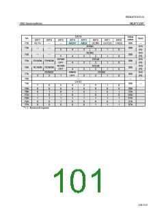
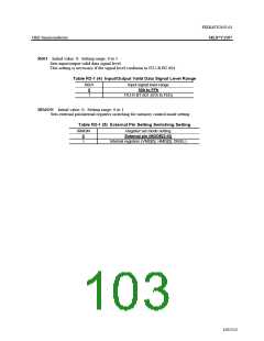
YBLS[1:0] Initial value: 00, Setting range: 00 to 11
Sets the luminance signal blanking level.
Used as the mask blanking level of the memory output disable data section.
Table R2-1 (3) Luminance Blanking Level Setting
YBLS
Luminance Blanking Level Setting
[1]
0
[0]
0
0 (00h) level
1 (01h) level
8 (08h) levels
16 (10h) levels
0
1
1
0
1
1
102/152

 OKI [ OKI ELECTRONIC COMPONETS ]