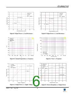
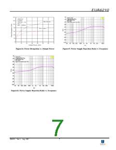
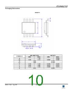
EUA6210
Amplifier Configuration Explanation
Application Information
As shown in Figure 1, the EUA6210 has three operational
amplifiers internally. Two of the amplifier’s have
externally configurable gain while the other amplifier is
internally fixed at the bias point acting as a unity-gain
buffer. The closed-loop gain of the two configurable
amplifiers is set by selecting the ratio of Rf to Ri.
Consequently, the gain for each channel of the IC is
Eliminating Output Coupling Capacitors
Typical single-supply audio amplifiers that drive single-
ended (SE) headphones use a coupling capacitor on each
SE output. This output coupling capacitor blocks the
half supply voltage to which the output amplifiers are
typically biased and couples the audio signal to the
headphones. The signal return to circuit ground is
through the headphone jack’s sleeve.
Av = −(R / R )
f
i
The EUA6210 eliminates these output coupling capacitors.
Amp3 is internally configured to apply a bandgap
referenced voltage (VREF = 1.58V) to a stereo headphone
jack’s sleeve. This voltage matches the quiescent voltage
present on the Amp1 and Amp2 outputs that drive the
headphones. The headphones operate in a manner similar
to a bridge-tied-load (BTL). The same DC voltage is
applied to both headphone speaker terminals. This results
in no net DC current flow through the speaker. AC current
flows through a headphone speaker as an audio signal’s
output amplitude increases on the speaker’s terminal.
The headphone jack’s sleeve is not connected to circuit
ground. Using the headphone output jack as a line-level
output will place the EUA6210’s bandgap referenced
voltage on a plug’s sleeve connection. This presents no
difficulty when the external equipment uses capacitively
coupled inputs. For the very small minority of equipment
that is DC coupled, the EUA6210 monitors the current
supplied by the amplifier that drives the headphone jack’s
sleeve. If this current exceeds 500mAPK, the amplifier is
shutdown, protecting the EUA6210 and the external
equipment.
By driving the loads through outputs VO1 and VO2 with
VO3 acting as a buffered bias voltage the EUA6210 does
not require output coupling capacitors. The typical
single-ended amplifier configuration where one side of
the load is connected to ground requires large, expensive
output coupling capacitors.
A configuration such as the one used in the EUA6210 has
a major advantage over single supply, single-ended
amplifiers. Since the outputs VO1, VO2, and VO3 are all
biased at VREF= 1.58V, no net DC voltage exists across
each load. This eliminates the need for output coupling
capacitors that are required in
a
single-supply,
single-ended amplifier configuration. Without output
coupling capacitors in
a
typical single-supply,
single-ended amplifier, the bias voltage is placed across
the load resulting in both increased internal IC power
dissipation and possible loudspeaker damage.
Current Limit Protection Circuitry
In order to limit excessive power dissipation in the load
when a shout-circuit occurs, the current limit in the load
is fixed to 250mA. The current in the output MOS
transistors is real-time monitored, and when exceeding
250mA, the gate voltage of the corresponding MOS
transistor is clipped and no more current can be delivered.
Eliminating the Half-Supply Bypass Capacitor
Typical single-supply audio amplifiers are normally
biased to1/2VDD in order to maximize the output swing of
the audio signal. This is usually achieved with a simple
resistor divider network from VDD to ground that provides
the proper bias voltage to the amplifier. However, this
scheme requires the use of a half-supply bypass capacitor
to improve the bias voltage’s stability and the amplifier’s
PSRR performance.
Micro Power Shutdown
The voltage applied to the SHUTDOWN pin controls the
EUA6210’s shutdown function. Activate micro-power
shutdown by applying a logic-low voltage to the
SHUTDOWN pin. When active, the EUA6210’s
micro-power shutdown feature turns off the amplifier’s
bias circuitry, reducing the supply current. The trigger
point is 0.4V(max) for a logic-low level, and 1.5v(min)for
a logic-high level. The low0.1µA (typ) shutdown current
is achieved by applying a voltage that is as near as ground
as possible to the SHUTDOWN pin. A voltage that is
higher than ground may increase the shutdown current.
There are a few ways to control the micro-power
shutdown. These include using a single-pole, single-throw
switch, a microprocessor, or a microcontroller. When
using a switch, connect a external 100kΩ pull-up resistor
between the SHUTDOWN pin and VDD. Connect the
switch between the SHUTDOWN pin and ground. Select
normal amplifier operation by opening the switch. Closing
the switch connects the SHUTDOWN pin to ground,
activating micro-power shutdown. The switch and resistor
The EUA6210 utilizes an internally generated, buffered
bandgap reference voltage as the amplifier’s bias voltage.
This bandgap reference voltage is not a direct function of
VDD and therefore is less susceptible to noise or ripple on
the power supply line. This allows for the EUA6210 to
have
a stable bias voltage and excellent PSRR
performance even without a half-supply bypass capacitor.
DS6210 Ver1.1 Aug. 2007
8

 EUTECH [ EUTECH MICROELECTRONICS INC ]