ESMT
M14D5121632A (2H)
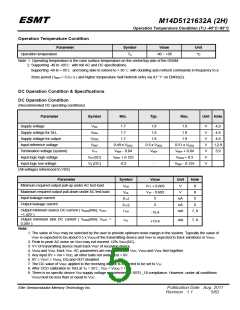
Operation Temperature Condition (TC) -40°C~95°C
Version
Unit
Parameter
Symbol
Test Condition
-1.8
-2.5
-3
t
CK = tCK (IDD);
Refresh command every tRFC (IDD) interval;
CKE is HIGH, CS is HIGH between valid commands;
Other control and address bus inputs are SWITCHING;
Data bus inputs are SWITCHING
Auto Refresh Current IDD5
150
110
100
mA
mA
Self Refresh Mode;
CLK and CLK at 0V; CKE ≤ 0.2V;
Other control and address bus inputs are FLOATING;
Data bus inputs are FLOATING
Self Refresh Current
IDD6
IDD7
10
All bank interleaving Reads, IOUT = 0mA;
BL = 4, CL= CL (IDD), AL = tRCD (IDD) – 1 × tCK (IDD);
t
t
CK = tCK (IDD), tRC = tRC (IDD),
RRD = tRRD (IDD), tRCD = 1 × tCK (IDD);
Operating Current
(Bank interleaving)
280
220
200
mA
CKE is HIGH, CS is HIGH between valid commands;
Address bus inputs are STABLE during Deslects;
Data pattern is the same as IDD4W;
Note:
1. IDD specifications are tested after the device is properly initialized.
2. Input slew rate is specified by AC Input Test Condition.
3. IDD parameters are specified with ODT disabled.
4. Data bus consists of DQ, DM, DQS and DQS , IDD values must be met with all combinations of EMRS bits 10 and 11.
5. Definitions for IDD:
LOW is defined as VIN ≤ VIL (AC) (max.).
HIGH is defined as VIN
VIH (AC) (min.).
STABLE is defined as inputs stable at a HIGH or LOW level.
FLOATING is defined as inputs at VREF = VDDQ/2
SWITCHING is defined as:
Address and control signal Inputs are changed between HIGH and LOW every other clock cycle (once per two clocks), and
DQ (not including mask or strobe) signal inputs are changed between HIGH and LOW every other data transfer (once per
clock).
6. When TC ≧ +85 ℃, IDD6 must be derated by 80%.
IDD6 will increase by this amount if TC ≧ +85 ℃ and double refresh option is still enabled.
7. AC Timing for IDD test conditions
For purposes of IDD testing, the following parameters are to be utilized.
-1.8
-2.5
-3
Parameter
CL (IDD)
Unit
DDR2-1066 (7-7-7)
DDR2-800 (5-5-5)
DDR2-667 (4-4-4)
7
13.125
58.125
10
5
12.5
57.5
10
4
tCK
ns
ns
ns
ns
ns
ns
ns
ns
ns
tRCD (IDD)
tRC (IDD)
12
57
10
50
3
tRRD (IDD)
tFAW (IDD)
tCK (IDD)
45
45
1.875
45
2.5
tRAS (IDD) min.
tRAS (IDD) max.
tRP (IDD)
45
45
70000
12.5
105
13.25
105
12
tRFC (IDD)
105
Elite Semiconductor Memory Technology Inc.
Publication Date : Aug. 2011
Revision : 1.1 7/62

 ESMT [ ELITE SEMICONDUCTOR MEMORY TECHNOLOGY INC. ]