ESMT
M14D5121632A (2H)
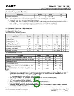
Operation Temperature Condition (TC) -40°C~95°C
Pin Description
Pin Name
Function
Pin Name
Function
Address inputs
- Row address A0~A12
DM is an input mask signal for write data.
LDM is DM for DQ0~DQ7 and UDM is DM
for DQ8~DQ15.
A0~A12,
BA0,BA1
DM
- Column address A0~A9
A10/AP : Auto Precharge
BA0, BA1 : Bank selects (4 Banks)
(LDM, UDM)
DQ0~DQ15
Data-in/Data-out
Differential clock input
CLK, CLK
CKE
Command input
Command input
Command input
Ground
Clock enable
RAS
CAS
Chip select
CS
VDDQ
VSSQ
VREF
Supply Voltage for DQ
Ground for DQ
Reference Voltage
WE
VSS
VDD
Power
DQS, DQS
Bi-directional differential Data Strobe.
VDDL
Supply Voltage for DLL
Ground for DLL
LDQS and LDQS are DQS for DQ0~DQ7;
UDQS and LDQS are DQS for DQ8~DQ15.
(LDQS, LDQS
UDQS, UDQS )
On-Die-Termination.
ODT is only applied to DQ0~DQ15, DM,
DQS and DQS .
ODT
NC
VSSDL
No connection
Absolute Maximum Rating
Parameter
Voltage on any pin relative to VSS
Voltage on VDD supply relative to VSS
Voltage on VDDL supply relative to VSS
Voltage on VDDQ supply relative to VSS
Storage temperature
Symbol
Value
Unit
VIN, VOUT
VDD
-0.5 ~ 2.3
-1.0 ~ 2.3
-0.5 ~ 2.3
-0.5 ~ 2.3
-55 ~ +100
V
V
VDDL
V
VDDQ
TSTG
V
°C ( Note *)
Stresses greater than those listed under “Absolute Maximum Ratings” may cause permanent damage to the device. This is a
stress rating only and functional operation of the device at these or any other conditions above those indicated in the operational
sections of this specification is not implied. Exposure to absolute maximum rating conditions for extended periods may affect
reliability.
Note *: Storage Temperature is the case surface temperature on the center/top side of the DRAM.
Elite Semiconductor Memory Technology Inc.
Publication Date : Aug. 2011
Revision : 1.1 4/62

 ESMT [ ELITE SEMICONDUCTOR MEMORY TECHNOLOGY INC. ]