ESMT
F25L04UA
Fast-Read (50 MHz ; 75 MHz; 100 MHz)
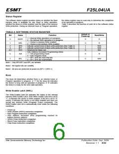
The High-Speed-Read instruction supporting up to 100 MHz is
initiated by executing an 8-bit command, 0BH, followed by
through all addresses until terminated by a low to high transition
on CE . The internal address pointer will automatically increment
until the highest memory address is reached. Once the highest
memory address is reached, the address pointer will
automatically increment to the beginning (wrap-around) of the
address space, i.e. for 4 Mbit density, once the data from address
location 07FFFFH has been read, the next output will be from
address location 000000H.
address bits [A23-A0] and a dummy byte. CE must remain
active low for the duration of the High-Speed-Read cycle. See
Figure 5 for the High-Speed-Read sequence.
Following a dummy byte (8 clocks input dummy cycle), the
High-Speed-Read instruction outputs the data starting from the
specified address location. The data output stream is continuous
CE
0
1 2
3
4 5 6 7
8
15 16
23 24
31 32
39 40
47 48
MODE3
MODE0
55 56
63 64
71 72
80
SCK
SI
0B
ADD.
MSB
ADD.
ADD.
X
MSB
N
N+1
DOUT
N+2
DOUT
N+3
DOU T
N+4
DOU T
HIGH IMPENANCE
SO
DOU T
MSB
Note : X = Dummy Byte : 8 Clocks Input Dummy (VIL or VIH)
Figure 5 : HIGH-SPEED-READ SEQUENCE
Elite Semiconductor Memory Technology Inc.
Publication Date: Sep. 2006
Revision: 1.1 9/24

 ESMT [ ELITE SEMICONDUCTOR MEMORY TECHNOLOGY INC. ]