ESMT
F25L04UA
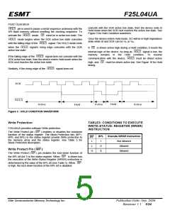
Status Register
The software status register provides status on whether the flash
memory array is available for any Read or Write operation,
whether the device is Write enabled, and the state of the memory
Write protection. During an internal Erase or Program operation,
the status register may be read only to determine the completion
of an operation in progress.
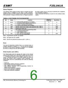
Table 4 describes the function of each bit in the software status
register.
TABLE 4: SOFTWARE STATUS REGISTER
Default at
Read/Write
Power-up
Bit
Name
BUSY
WEL
Function
1 = Internal Write operation is in progress
0 = No internal Write operation is in progress
1 = Device is memory Write enabled
0 = Device is not memory Write enabled
Indicate current level of block write protection (See Table 5)
Indicate current level of block write protection (See Table 5)
Reserved for future use
0
0
0
R
R
1
2
3
4:5
BP0
BP1
RES
1
1
0
R/W
R/W
N/A
Auto Address Increment Programming status
1 = AAI programming mode
0 = Byte-Program mode
1 = BP1, BP0 are read-only bits
0 = BP1, BP0 are read/writable
6
7
AAI
0
0
R
BPL
R/W
Note1 : Only BP0,BP1 and BPL are writable
Note2 : All register bits are volatility
Note3 : All area are protected at power-on (BP1=1,BP0=1)
Busy
The Busy bit determines whether there is an internal Erase or
Program operation in progress. A “1” for the Busy bit indicates
the device is busy with an operation in progress. A “0” indicates
the device is ready for the next valid operation.
Write Enable Latch (WEL)
The Write-Enable-Latch bit indicates the status of the internal
memory Write Enable Latch. If the Write-Enable-Latch bit is set to
“1”, it indicates the device is Write enabled. If the bit is set to “0”
(reset), it indicates the device is not Write enabled and does not
accept any memory Write (Program/ Erase) commands. The
Write-Enable-Latch bit is automatically reset under the following
conditions:
• Power-up
• Write-Disable (WRDI) instruction completion
• Byte-Program instruction completion
• Auto Address Increment (AAI) programming reached its
highest memory address
• Sector-Erase instruction completion
• Block-Erase instruction completion
• Chip-Erase instruction completion
Elite Semiconductor Memory Technology Inc.
Publication Date: Sep. 2006
Revision: 1.1 6/24

 ESMT [ ELITE SEMICONDUCTOR MEMORY TECHNOLOGY INC. ]