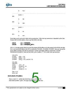
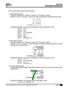
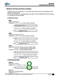
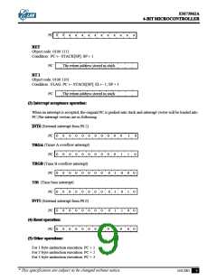
EM73962A
4-BIT MICROCONTROLLER
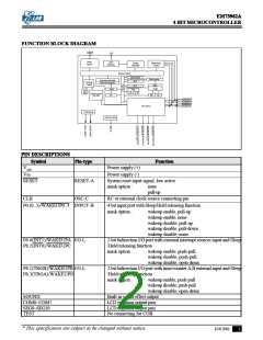
FUNCTION BLOCK DIAGRAM
RESET
CLK
Reset
Control
Clock
Generator
Sleep Mode
Control
Timing
Generator
System Control
Data pointer
ACC
Stack pointer
Instruction Decoder
Instruction Register
Interrupt
Control
Stack
ROM
ALU
Flag
ROM
Time
Base
Z
C
S
Timer/Counter
(TA,TB)
PC
HR
LR
P0.0/WAKEUP0
P0.1/WAKEUP1
P0.2/WAKEUP2
P0.3/WAKEUP3
I/O Control
LCD Driver
SOUND GEN.
PIN DESCRIPTIONS
Symbol
VDD
Pin-type
Function
Power supply (+)
Power supply (-)
Vss
RESET
RESET-A
OSC-C
System reset input signal, low active
mask option :
none
pull-up
CLK
RC or external clock source connecting pin
P0.(0..3)/WAKEUP0..3 INPUT-B
4-bit input port with Sleep/Hold releasing function
mask option :
wakeup enable, pull-up
wakeup enable, none
wakeup disable, pull-up
wakeup disable, pull-down
wakeup disable, none
P8.0(INT1)/WAKEUPA I/O-L
P8.2(INT0)/WAKEUPC
2-bit bidirection I/O port with external interrupt sources input and Sleep
/Hold releasing function
mask option :
wakeup enable, push-pull
wakeup disable, push-pull
wakeup disable, open-drain
P8.1(TRGB)/WAKEUPB I/O-L
P8.3(TRGA)/WAKEUPD
2-bit bidirection I/O port with time/counter A,B external input and Sleep
/Hold releasing function
mask option :
wakeup enable, push-pull
wakeup disable, push-pull
wakeup disable, open-drain
SOUND
Built-in sound effect output
LCD common output pins
LCD segment output pins
No connecting for COB
COM0~COM7
SEG0~SEG39
TEST
* This specification are subject to be changed without notice.
10.8.2001
2

 ELAN [ ELAN MICROELECTRONICS CORP ]