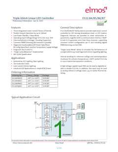
Triple 60mA Linear LED Controller
Preliminary Information - Jan 21, 2015
E522.84/85/86/87
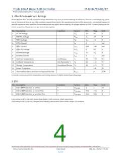
1 Absolute Maximum Ratings
Stresses beyond these absolute maximum ratings listed below may cause permanent damage to the device. These are stress ratings only; opera-
tion of the device at these or any other conditions beyond those listed in the operational sections of this document is not implied. Exposure to
absolute maximum rated conditions for extended periods may affect device reliability. All voltages referred to VGND. Currents flowing into ter-
minals are positive, those drawn out of a terminal are negative.
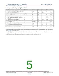
No. Description
Condition
Symbol
Min
Max
Unit
1
2
3
4
5
6
7
8
9
VS Pin Voltage
ENA Pin Voltage
IR Pin Voltage
VVS
-0.3
40
V
VENA
VIR
-0.3
-0.3
-1
40
5.5
1
V
V
IR Pin Current
IIR
mA
mA
V
LEDx Current
ILED.x
VLED,x
VRUN
IRUN
TJ
-100
-1
100
VVS
VVS
5
LEDx Pin Voltage
RUN Pin Voltage
RUN Pin Current
Junction Temperature
-0.3
-5
V
mA
°C
Continuous
-40
-40
-40
150
125
125
1.8
8
10 Ambient Temperature
Info Parameter 1)
TA
°C
11 Storage Temperature
Unsoldered Device TST
PV
°C
12 Power Dissipation
W
13 Thermal Resistance Junction to Exposed Die Pad
RTH,J-C
K/W
1) consider maximum junction temperature and cooling measures to define ambient operating range
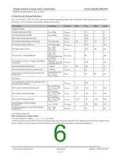
2 ESD
No. Description
Condition
Symbol
Min
Max
Unit
1)
1
2
3
ESD HBM Protection at all Pins
VESD,HBM
-2
2
kV
2)
2)
ESD CDM Protection at Corner Pins
ESD CDM Protection at all other Pins
VESD,CDM,1
VESD,CDM,2
-750
-500
750
500
V
V
1) According to AEC-Q 100-002, Human Body Model, 1.5kΩ resistance, 100pF capacitance.
2) According to AEC-Q 100-011, Charged Device Model, pulse rise time (10% to 90%) <400ps, 1Ω resistance.
This document contains information on a pre-production product. Elmos Semiconductor AG reserves the right to change specifications and information herein without notice.
Elmos Semiconductor AG
Data Sheet
QM-No.: 25DS0137E.00
4/20

 ELMOS [ ELMOS SEMICONDUCTOR AG ]