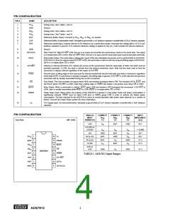
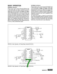
PIN CONFIGURATION
PIN #
NAME
DESCRIPTION
1
2
3
4
5
6
7
R1IN
GND
R2IN
R3IN
BUF
CAP
REF
Analog Input. See Tables I and IV.
Ground
Analog Input. See Tables I and IV.
Analog Input. See Tables I and IV.
Reference Buffer Output. Connect to R1IN, R2IN, or R3IN, as needed.
Reference Buffer Compensation Node. Decouple to ground with a 1µF tantalum capacitor in parallel with a 0.01µF ceramic capacitor.
Reference Input/Output. Outputs internal +2.5V reference via a series 4kΩ resistor. Decouple this voltage with a 1µF to 2.2µF
tantalum capacitor to ground. If an external reference voltage is applied to this pin, it will override the internal reference.
8
9
GND
Ground
DATACLK
Data Clock Pin. With EXT/INT LOW, this pin is an output and provides the synchronous clock for the serial data. The output
is tri-stated when CS is HIGH. With EXT/INT HIGH, this pin is an input and the serial data clock must be provided externally.
10
11
12
DATA
EXT/INT
CONV
Serial Data Output. The serial data is always the result of the last completed conversion and is synchronized to DATACLK.
If DATACLK is from the internal clock (EXT/INT LOW), the serial data is valid on both the rising and falling edges of DATACLK.
DATA is tri-stated when CS is HIGH.
External or Internal DATACLK Pin. Selects the source of the synchronous clock for serial data. If HIGH, the clock must be
provided externally. If LOW, the clock is derived from the internal conversion clock. Note that the clock used to time the
conversion is always internal regardless of the status of EXT/INT.
Convert Input. A falling edge on this input puts the internal sample/hold into the hold state and starts a conversion regardless
of the state of CS. If a conversion is already in progress, the falling edge is ignored. If EXT/INT is LOW, data from the previous
conversion will be serially transmitted during the current conversion.
13
14
15
CS
Chip Select. This input tri-states all outputs when HIGH and enables all outputs when LOW. This includes DATA, BUSY, and
DATACLK (when EXT/INT is LOW). Note that a falling edge on CONV will initiate a conversion even when CS is HIGH.
BUSY
PWRD
Busy Output. When a conversion is started, BUSY goes LOW and remains LOW throughout the conversion. If EXT/INT is
LOW, data is serially transmitted while BUSY is LOW. BUSY is tri-stated when CS is HIGH.
Power Down Input. When HIGH, the majority of the ADS7813 is placed in a low power mode and power consumption is
significantly reduced. CONV must be taken LOW prior to PWRD going LOW in order to achieve the lowest power
consumption. The time required for the ADS7813 to return to normal operation after power down depends on a number of
factors. Consult the Power Down section for more information.
16
VS
+5V Supply Input. For best performance, decouple to ground with a 0.1µF ceramic capacitor in parallel with a 10µF tantalum
capacitor.
PIN CONFIGURATION
ANALOG
INPUT
RANGE (V)
CONNECT
R1IN
CONNECT
R2IN
CONNECT
R3IN
INPUT
IMPEDANCE
(kΩ)
Top View
DIP, SOIC
TO
TO
TO
±10V
VIN
BUF
GND
45.7
0.3125V to
2.8125V
VIN
GND
BUF
BUF
VIN
VIN
BUF
GND
VIN
VIN
VIN
> 10,000
26.7
±5V
R1IN
GND
R2IN
R3IN
BUF
CAP
REF
GND
1
2
3
4
5
6
7
8
16 VS
15
0V to 10V
0V to 4V
±3.33V
VIN
26.7
GND
VIN
21.3
PWRD
BUF
21.3
14 BUSY
13 CS
0.5V to
4.5V
GND
VIN
GND
21.3
ADS7813
12 CONV
11 EXT/INT
10 DATA
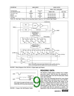
TABLE I. ADS7813 Input Ranges.
9
DATACLK
®
ADS7813
4

 BB [ BURR-BROWN CORPORATION ]