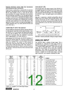
DIGITAL OUTPUT
DESCRIPTION
ANALOG INPUT
BINARY TWO’S COMPLEMENT
Full-Scale Range
±10V
0.5V to 4.5V
Least Significant Bit (LSB)
305µV
61µV
BINARY CODE
HEX CODE
+Full Scale –1LSB
Midscale
9.999695V
0V
4.499939V
2.5V
0111 1111 1111 1111
0000 0000 0000 0000
1111 1111 1111 1111
10000 0000 0000 0000
7FFF
0000
FFFF
8000
Midscale –1LSB
–Full Scale
–305µV
–10V
2.499939µV
0.5V
TABLE III. Ideal Input Voltage and Corresponding Digital Output for Two Common Input Ranges.
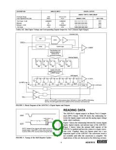
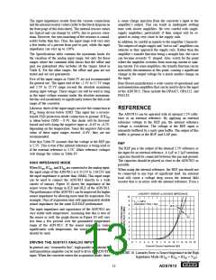
Converter Core
REF
CDAC
CONV
Clock
Control Logic
BUSY
Each flip-flop in the
working register is
latched as the
conversion proceeds
Working Register
D Q
D
Q
D
Q
D
Q
D
Q
• • •
W0
W1
W2
W14
W15
Update of the shift
register occurs just prior
to BUSY Rising(1)
Shift Register
DATA
D
Q
D
Q
D
Q
D
Q
D
Q
D
Q
EXT/INT
S0
S1
S2
S14
S15
SOUT
Delay
DATACLK
CS
NOTE: (1) If EXT/INT is HIGH (external clock), DATACLK is HIGH, and CS is LOW during
this time, the shift register will not be updated and the conversion result will be lost.
FIGURE 3. Block Diagram of the ADS7813’s Digital Inputs and Outputs.
READING DATA
The ADS7813’s digital output is in Binary Two’s Comple-
ment (BTC) format. Table III shows the relationship be-
tween the digital output word and the analog input voltage
under ideal conditions.
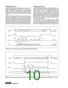
CONV
BUSY
t25
t6 – t25
Figure 3 shows the relationship between the various digital
inputs, digital outputs, and internal logic of the ADS7813.
Figure 4 shows when the internal shift register of the
ADS7813 is updated and how this relates to a single conver-
sion cycle. Together, these two figures point out a very
important aspect of the ADS7813: the conversion result is
not available until after the conversion is complete. The
implications of this are discussed in the following sections.
NOTE: Update of the internal shift register occurs in the
shaded region. If EXT/INT is HIGH, then DATACLK
must be LOW or CS must be HIGH during this time.
FIGURE 4. Timing of the Shift Register Update.
®
9
ADS7813

 BB [ BURR-BROWN CORPORATION ]