CHAPTER 4 PIN FUNCTION (µPD78070AY)
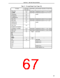
4.1 Pin Function List
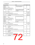
(1) Port pins (1/2)
Pin Name Input/Output
Function
After Reset Alternate Function
P00
P01
Input
Input only
Input
INTP0/TI00
INTP1/TI01
INTP2
Input/output mode can be specified
bit-wise.
P02
P03
Input/
Port 0.
If used as an input port, an on-chip
INTP3
Input
P04
output
8-bit input/output port.
pull-up resistor can be connected
by software.
INTP4
P05
INTP5
P06
INTP6
P07Note 1
P10 to P17
Input
Input only
Input
Input
XT1
Port 1.
8-bit input/output port.
Input/
Input/output mode can be specified bit-wise.
ANI0 to ANI7
output
If used as an input port, an on-chip pull-up resistor can be connected by
softwareNote 2
.
P20
P21
P22
P23
P24
P25
P26
P27
P30
P31
P32
P33
P34
P35
P36
P37
SI1
SO1
Port 2.
SCK1
STB
Input/
8-bit input/output port.
Input
output
Input/output mode can be specified bit-wise.
If used as an input port, an on-chip pull-up resistor can be connected by
software.
BUSY
SI0/SB0/SDA0
SO0/SB1/SDA1
SCK0/SCL
TO0
TO1
Port 3.
TO2
Input/
8-bit input/output port.
TI1
Input
output
Input/output mode can be specified bit-wise.
If used as an input port, an on-chip pull-up resistor can be connected by
software.
TI2
PCL
BUZ
—
Notes 1. When the P07/XT1 pin is used as an input port, set the bit 6 (FRC) of the processor clock control
register (PCC) to 1 (do not use the feedback resistor internal to the subsystem clock oscillator).
2. When pins P10/ANI0 to P17/ANI7 are used as an analog input of the A/D converter, set port 1 to
the input mode. The on-chip pull-up resistor is automatically disabled.
71

 ETC [ ETC ]