CHAPTER 3 PIN FUNCTION (µPD78070A)
3.2.10 P130, P131 (Port 13)
These are 2-bit input/output ports. Besides serving as input/output ports, they are used for D/A converter analog
output.
The following operating modes can be specified bit-wise.
(1) Port mode
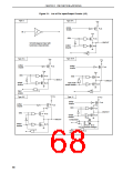
These ports function as 2-bit input/output ports. They can be specified bit-wise as input or output ports with
port mode register 13 (PM13). When they are used as input ports, on-chip pull-up resistors can be connected
by defining the pull-up resistor option register H (PUOH).
(2) Control mode
These ports function as D/A converter analog output (ANO0 and ANO1).
Caution When only either one of the D/A converter channels is used with AVREF1 < VDD, the other pins
that are not used as analog outputs must be set as follows:
•
Set PM13× bit of the port mode register 13 (PM13) to 1 (input mode) and connect the pin
to VSS.
•
Set PM13× bit of the port mode register 13 (PM13) to 0 (output mode) and the output latch
to 0, to output low level from the pin.
3.2.11 AD0 to AD7
These are the low-order address/data bus pins for external memory.
3.2.12 A0 to A15
These are the address bus pins for external memory.
3.2.13 RD
This is a strobe signal output pin for read operation from external memory.
3.2.14 WR
This is a strobe signal output pin for write operation from external memory.
3.2.15 ASTB
This is a strobe signal output pin that externally latches the address data from the AD0 to AD7, A0 to A15 pins
in order to access the external memory.
In the case of the µPD78070A, this signal does not need to be used because the external device expansion function
is fixed at the separate bus mode, but the address strobe signal is being output.
3.2.16 AVREF0
A/D converter reference voltage input pin.
When A/D converter is not used, connect this pin to VSS.
3.2.17 AVREF1
D/A converter reference voltage input pin.
When D/A converter is not used, connect this pin to VDD.
3.2.18 AVDD
This is an analog power supply pin of A/D converter. Always use the same voltage as that of the VDD pin even
when not using A/D converter.
64

 ETC [ ETC ]