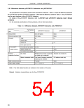
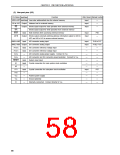
CHAPTER 3 PIN FUNCTION (µPD78070A)
(2) Non-port pins (2/2)
Pin Name Input/Output
Function
After Reset Alternate Function
AD0 to AD7 Input/Output Low-order address/data bus for external memory
A0 to A15 Output Address bus for external memory
Input
Input
Input
—
—
—
RD
WR
Output Strobe signal output for read operation from external memory
Strobe signal output for write operation from external memory
WAIT
ASTB
Input
Wait insertion when accessing external memory
Input
Input
P66
—
Output Strobe output externally latching address information output to AD0 to
AD7 and A0 to A15 to access external memory
ANI0 to ANI7 Input
A/D converter analog input
Input
Input
—
P10 to P17
ANO0, ANO1 Output D/A converter analog output
P130, P131
AVREF0
AVREF1
AVDD
AVSS
RESET
X1
Input
Input
—
A/D converter reference voltage input
—
—
D/A converter reference voltage input
—
A/D converter analog power supply. Connect to VDD.
A/D converter and D/A converter ground potential. Connect to VSS.
System reset input
—
—
—
—
—
Input
Input
—
—
—
Crystal connection for main system clock oscillation
—
—
X2
—
—
XT1
XT2
VDD
Input
—
Crystal connection for subsystem clock oscillation
Input
—
P07
—
—
Positive power supply
—
—
VSS
—
Ground potential
—
—
IC
—
Internally connected. Connect directly to VSS.
—
—
58

 ETC [ ETC ]