CHAPTER 1 OUTLINE (µPD78070A)
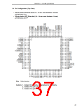
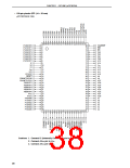
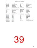
A0 to A15
AD0 to AD7
ANI0 to ANI7
ANO0, ANO1
ASCK
: Address Bus
P130, P131
PCL
: Port 13
: Address/Data Bus
: Analog Input
: Analog Output
: Asynchronous Serial Clock
: Address Strobe
: Analog Power Supply
: Analog Reference Voltage
: Analog Ground
: Busy
: Programmable Clock
: Read Strobe
: Reset
RD
RESET
RTP0 to RTP7
RxD
: Real-time Output Port
: Receive Data
: Serial Bus
ASTB
AVDD
SB0, SB1
SCK0 to SCK2
SI0 to SI2
SO0 to SO2
STB
AVREF0, AVREF1
AVSS
: Serial Clock
: Serial Input
: Serial Output
: Strobe
BUSY
BUZ
: Buzzer Clock
: Internally Connected
: Interrupt from Peripherals
: Port 0
IC
TI00, TI01
TI1, TI2, TI5, TI6
: Timer Input
: Timer Input
INTP0 to INTP6
P00 to P07
P10 to P17
P20 to P27
P30 to P37
P60 to P63, P66
P70 to P72
P90 to P96
P100 to P103
P120 to P127
TO0 to TO2, TO5, TO6 : Timer Output
: Port 1
TxD
: Transmit Data
: Power Supply
: Ground
: Port 2
VDD
: Port 3
VSS
: Port 6
WAIT
WR
: Wait
: Port 7
: Write Strobe
: Port 9
X1, X2
XT1, XT2
: Crystal (Main System Clock)
: Crystal (Subsystem Clock)
: Port 10
: Port 12
39

 ETC [ ETC ]