TEA1716T
NXP Semiconductors
Resonant power supply control IC with PFC
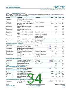
Table 7.
Characteristics …continued
Tamb = 25 C; VSUPIC = 20 V; VSUPHV > 40 V; all voltages are measured with respect to SGND; currents are positive when
flowing into the IC; unless otherwise specified.
Symbol
Parameter
high frequency CMR current on pin VSSHBC < Vss(lf-hf)(SSHBC)
SSHBC discharge only
low frequency CMR current on pin VSSHBC > Vss(lf-hf)(SSHBC)
Conditions
Min
Typ
Max Unit
Icmr(hf)(SSHBC)
-
1800
-
A
Icmr(lf)(SSHBC)
-
440
-
A
SSHBC
HBC high frequency sensing, HFP - HBC
Vhfp High-frequency protection voltage
discharge only
[2]
across resistor Rfmax
1.70 1.83
2.00
V
HBC overcurrent sensing, OCR/OCP - HBC (pin SNSCURHBC)
Vocr(HBC)
HBC overcurrent regulation voltage
positive level;
HS on + HS-LS non-overlap
time
0.45 +0.50 0.55
V
V
negative level;
LS on + LS-HS non-overlap
time
0.55 0.50 0.45
Vocp(HBC)
HBC overcurrent protection voltage
positive level;
HS on + HS-LS non-overlap
time
-
-
+1.75
-
-
V
V
negative level;
LS on + LS-HS non-overlap
time
1.75
Ibstc(SNSCURHBC)max
maximum boost compensation
current on pin SNSCURHBC
VSNSBOOST = 1.8 V
source current;
-
-
170
-
-
A
A
VSNSCURHBC = 0.5 V
sink current;
170
VSNSCURHBC = 0.5 V
HBC Capacitive Mode Protection (CMP) (pin HB)
tto(cmr) time-out capacitive mode regulation
-
690
-
ns
[1] The marked levels on this pin are correlated. The voltage difference between the levels has much less spread than the absolute value of
the levels themselves.
[2] Switching level has some hysteresis. The hysteresis falls within the limits.
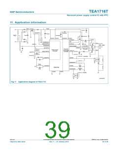
[3] For a typical application with a compensation network on pin COMPPFC, like the example in Figure 17.
[4] Minimum required voltage change time for valley recognition on pin SNSAUXPFC.
[5] Minimum time required between demagnetization detection and V/t = 0 on pin SNSAUXPFC.
TEA1716T
All information provided in this document is subject to legal disclaimers.
© NXP B.V. 2012. All rights reserved.
Objective data sheet
Rev. 1 — 27 January 2012
38 of 46

 ETC [ ETC ]