SigmaTel, Inc.
Data Sheet
STAC9721
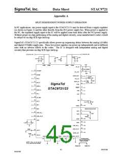
Appendix A
SPLIT INDEPENDENT POWER SUPPLY OPERATION
In PC applications, one power supply input to the STAC9721/23 may be derived from a supply regulator
(as shown in Figure 3) and the other directly from the PCI power supply bus. When power is applied to
the PC, the regulated supply input to the IC will be applied some time delay after the PCI power supply.
Without proper on-chip partitioning of the analog and digital circuitry, some manufacturer's codecs would
be subject to on-chip SCR type latch-up.
SigmaTel’s STAC9721/23 specifically allows power-up sequencing delays between the analog (AVddx)
and digital (VDddx) supply pins. These two power supplies can power-up independently and at different
rates with no adverse effects to the codec. The IC is designed with independent analog and digital
circuitry that prevents on-chip SCR type latch-up.
.
3.3V or 5V ± 5%
3.3V or 5V ± 5%
0.1uF
0.1uF
0.1uF
10uF
0.1uF
1uF
25
38
AVdd2
1
9
27pF
AVdd1
DVdd1
DVdd2
2
3
XTL_IN
24.576MHz
27pF
12
_
PC BEEP
XTL_OUT
13
14
PHONE
AUX_L
5
6
SDATA_OUT
BIT_CLK
SDATA_IN
SYNC
22 ohms
8
27pF
EMI
Filter
15
16
AUX_R
10
SigmaTel
STAC9721/23
VIDEO_L
11
45
RESET
CID0
17
18
VIDEO_R
CD_L
46
CID1
19
20
CD_GND
CD_R
27
28
Vref
0.1uF
1uF
21
22
23
MIC1
Vrefout
MIC2
Optional Anti-Pop Circuit
31
33
CAP1
CAP3
LINE_IN_L
LINE_IN_R
10uF
24
32
100uF
34
APOP
CAP2
47
35
EAPD
0.1uF
1uF
LINE_OUT_L
36
37
LINE_OUT_R
MONO_OUT
820pF
29
30
AFILT1
AFILT2
820pF
AVss2
42
DVss1
4
DVss2 LNLVL_OUT_L
LNLVL_OUT_R
41
AVss1
26
** Teminate ground
plane as close to power
supply as possible
39
7
NOTE: Pins 31, 33, 34, 40
43, 44, and 48 are No Connects
Analog Gnd
Digital Gnd
45
04/07/00
04/07/00

 ETC [ ETC ]