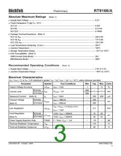
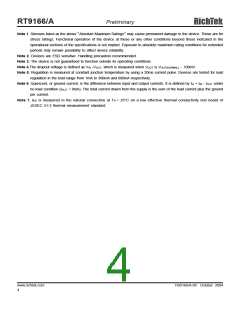
Preliminary
RT9166/A
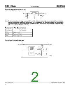
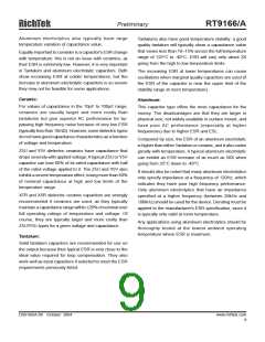
Typical Application Circuit
RT9166/A
V
VIN
VOUT
GND
V
IN
OUT
C
C
OUT
IN
1uF
1uF
Note: To prevent oscillation, a 1µF minimum X7R or X5R dielectric is strongly recommended if ceramics are
used as input/output capacitors. When using the Y5V dielectric, the minimum value of the input/output
capacitance that can be used for stable over full operating temperature range is 3.3µF. (see Application
Information Section for further details)
Functional Pin Description
Pin Name
Pin Function
VIN
Supply Input
VOUT
GND
Regulator Output
Common Ground
Function Block Diagram
VIN
VOUT
Error
Amplifier
Current
Limiting
Sensor
-
Thermal
Shutdown
1.2V
Reference
GND
www.richtek.com
2
DS9166/A-09 October 2004

 ETC [ ETC ]